Mosfet
Found 9 free book(s)
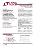
LTC4441/LTC4441-1 - N-Channel MOSFET Gate Driver
www.analog.comLTC4441/LTC4441-1 1 44411fa Typical applicaTion FeaTures DescripTion N-Channel MOSFET Gate Driver The LTC®4441/LTC4441-1 is an N-channel MOSFET gate driver that can supply up to 6A of peak output current.
A MOSFETPowerAmplifier with ErrorCorre - …
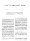
www.cordellaudio.comPAPERS MOSFET POWER AMPLIFIER WITH ERRORCORRECTION MOSFET is made possible by many of the same ad- tically from the drain contact on the back of the chip
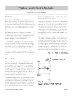
Practical Mosfet Testing for Audio - FIRST WATT
www.firstwatt.comPractical Mosfet Testing for Audio page 2 out the Drain. This connection has no current gain - the output current equals the input current. It can produce
AN-1645 LM4702 Driving a MOSFET Output Stage …
www.ti.comwww.ti.com MOSFET Amplifier Design The MOSEFET devices listed in Table 1 are devices from three suppliers that will meet the design criteria based on the LM4702 limitations for direct drive and the target output power specification into a resistive
Fundamentals of MOSFET and IGBT Gate Driver …
www.ti.comSLUA618–March 2017–Revised SLUP169 – April 2002 1 Submit Documentation Feedback Copyright © 2017–2002, Texas Instruments Incorporated Fundamentals of MOSFET and IGBT Gate Driver Circuits
LTC4446 - High Voltage High Side / Low Side N …
www.analog.comLTC4446 1 4446f TYPICAL APPLICATION FEATURES APPLICATIONS DESCRIPTION High Voltage High Side/ Low Side N-Channel MOSFET Driver The LTC ®4446 is a high frequency high voltage gate driver
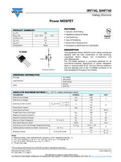
Power MOSFET - Vishay
www.vishay.comwww.vishay.com Document Number: 91054 2 S11-0507-Rev. C, 21-Mar-11 This datasheet is subject to change without notice. THE PRODUCT DESCRIBED HERE IN AND THIS DATASHEET ARE SUBJECT TO SPECIFIC DISCLAIMERS, SET FORTH AT www.vishay.com/doc?91000
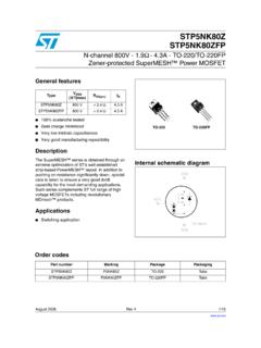
N-channel 800V - 1.9 - 4.3A - TO-220/TO-220FP …
www.st.comAugust 2006 Rev 4 1/15 15 STP5NK80Z STP5NK80ZFP N-channel 800V - 1.9Ω - 4.3A - TO-220/TO-220FP Zener-protected SuperMESH™ Power MOSFET General features

avalanche performance. - redrok.com
www.redrok.com4 www.irf.com Fig 8. Maximum Safe Operating Area Fig 6. Typical Gate Charge Vs. Gate-to-Source Voltage Fig 5. Typical Capacitance Vs. Drain-to-Source Voltage