Search results with tag "Mosfets"
Depletion-Mode Power MOSFETs and ... - IXYS Corporation
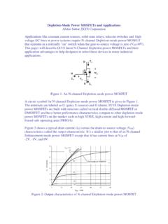
www.ixys.comIXYS Depletion-mode power MOSFETs are built with structure called vertical double-diffused MOSFET or DMOSFET and have better performance characteristics compare to other depletion-mode power MOSFETs on the market such as high VDSX, high current and high forward-biased safe operating area (FBSOA).

Chapter 9: FET Amplifiers And Switching Circuits
staff-old.najah.eduCircuit: where switch MOSFETs with a capacitor can be used to replace a resistor 9-5: MOSFET Digital Switching MOSFETs are also used in switching applications in digital integrated circuits CMOS (Complementary MOS) CMOS combines n-channel and/or p-channel E-MOSFETs in a series arrangement. The shown figure represent a logic Inverter Gate
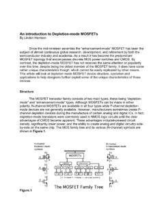
An introduction to Depletion-mode MOSFETs
aldinc.comdealing with depletion-mode MOSFETs will be straightforward. A few characteristics that may be a bit confusing are: 1. Drain saturation current - IDSS With an enhancement-mode MOSFET this is a leakage current. With a depletion-mode MOSFET it is the maximum limiting current that can flow between the drain and
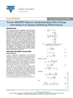
Power MOSFET Basics: Understanding Gate Charge and …
www.vishay.comVISHAY SILICONIX Power MOSFETs Device Application Note AN608A Power MOSFET Basics: Understanding Gate Charge and Using it to Assess Switching Performance www.vishay.com APPLICATION NOTE Revision: 16-Feb-16 1 Document Number: 73217 For technical questions, contact: pmostechsupport@vishay.com THIS DOCUMENT IS SUBJECT …

Power MOSFET - Vishay Intertechnology
www.vishay.comThird generation Power MOSFETs from Vishay provide the designer with the best combination of fast switching, ruggedized device design, low on-resistance and cost-effectiveness. The TO-247 package is preferred for commercial-industrial applications where higher power levels preclude the use of TO-220 devices. The TO-247 is similar but superior ...

LTC1144 - Switched-Capacitor Wide Input Range Voltage ...
www.analog.comvoltage level shifter, and four power MOSFETs. A special logic circuit will prevent the power N-channel switch substrate from turning on. applicaTions n Wide Operating Supply Voltage Range: 2V to 18V n Boost Pin (Pin 1) for Higher Switching Frequency n Simple Conversion of 15V to –15V Supply n Low Output Resistance: 120Ω Maximum

APPLICATION NOTE - MIT
web.mit.eduThe output stage is implemented either with two N-Channel MOSFETs in totem pole configuration (source follower as a current sou rce and common source for current sinking), or with an N-Channel and a P-Channel CMOS inverter stage. Each MOSFET can sink or sourc e gate currents from 0.12 to 2A, depending on the MGD.
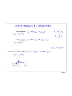
MOSFET transistor I-V characteristics
course.ece.cmu.eduMOSFET transistor I-V characteristics iD K 2()vGS–Vt vDS vDS ... • But for ICs we can assume that there can be a positive VSB for NMOSFETs VS2>0 VS1B=0 VB VS2B=0 VS1B=0 VS2B>0. Lecture 20-4 Body Effect
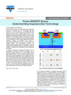
Power MOSFET Basics Understanding Superjunction …
www.vishay.com600 V rated MOSFETs, more than 95 % of the resistance comes from the epitaxial layer. It is obvious that for any significant reduction in the RDS(on) value, it is necessary to find a way of heavily doping the drift region and drastically reducing the epi resistance. N - Epi N + N + Substrate P + Body Oxide Oxide Gate Source and Body Source and ...

RF Power LDMOS Transistors High Ruggedness N--Channel ...
www.nxp.comEnhancement--Mode Lateral MOSFETs These devices are designed for use in HF and VHF communications, industrial, scientific and medical (ISM) and broadcast and aerospace applications. The devices are extremely rugged and exhibit high performance up to 250 MHz. Typical Performance: VDD =50Vdc Frequency (MHz) Signal Type Pout (W) Gps (dB) D (%) 13 ...

Power MOSFET Selection Guide - NXP
www.nxp.comA MOSFET’s RDSon is given by the formula: RDSon = Rchannel + Rdrift + Rsubstrate + (Rpackage) Many manufacturers focus on reducing Rchannel to drive RDSon down. NXP’s Super-junction allows for an optimisation of all 3 components for reduction in RDSon, whilst also enhancing switching performance and Safe Operating Area. Maximising Switching ...

2. 最先端FinFETプロセス・集積化技術
www.journal.ieice.org要である.また平面形MOSFETと同様にソース・ドレー ン部にSiGe,SiC等を用いることでチャネル部に応力 を印加できて,キャリヤ移動度を改善できる可能性も示 唆されている().一方,低抵抗金属のソース・ドレーン

空調機用モータ・インバータの最新技術
www.giho.mitsubishielectric.co.jp回路にsic-ダイオード及びsic-mosfetを適用して,エ アコンの電力損失を低減してきた。今回,業界で初めて(注1) 店舗・事務所向けの業務用パッケージエアコンの圧縮機 モータ駆動用インバータにsic -mosfetを搭載したフ ルsic-dipipmを採用した(図6)。

© No. 60AP001E Rev.0012017 ROHM Co., Ltd. Application …
fscdn.rohm.com近年、sic mosfet は、様々な電源アプリケーションや電力ラインのスイッチング素子として急激に使用が加速しています。 これは従来のパワー 半導体と比較して高速スイッチング動作が可能となったことがひとつの要因となっていますが、スイッチング時の ...

CAB011M12FM3 VDS Half-Bridge Module RDS(on)
assets.wolfspeed.com• Zero Turn-Off Tail Current from MOSFET • Normally-Off, Fail-Safe Device Operation V DS 1200 V R DS(on) 11 mΩ System Benefits • Enables Compact, Lightweight Systems • Increased System Efficiency due to Low Switching & Conduction Losses of SiC • Reduced Thermal Requirements and System Cost Applications • EV Chargers • Solar
Totem-pole PFC reference design with SiC technology
www.st.comSilicon carbide MOSFET 650 V, 45 A TN3050H-12WY SCR Thyristor 30A 1200V 1200V 600V 600V 1200V STM32F334 VIPer26LD 97.5 % efficiency at full load Key Products: SCTW35N65G2V (SiC MOSFET) TN3050H-12GY (SCR Thyristor) STGAP2AS (Galvanic insulated gate driver) STM32F334 (32-bit MCU) VIPer26LD (converter for aux. PS)

LTC3895 - 150V Low Iq, Synchronous Step-Down DC/DC …
www.analog.com150V Low IQ, Synchronous Step-Down DC/DC Controller The LTC®3895 is a high performance step-down switching regulator DC/DC controller that drives an all N-channel synchronous power MOSFET stage that can operate from input voltages up to 140V. A constant frequency current mode architecture allows a phase-lockable frequency of up to 850kHz.

Power MOSFET avalanche characteristics and ratings
www.st.comwas quite simple: the vertical MOSFET structure has an integral body drain diode which cannot be eliminated. By changing some process and layout parameters, it is possible to guarantee the use of the clamping capability of this diode for withstanding accidental voltage/power surges beyond the nominal drain source voltage.
Design Guide for QR Flyback Converter - Mouser Electronics
www.mouser.comthe MOSFET. Whenever VR is less than or equal to VIN, ZVS condition can be achieved. However as the input voltage increases ZVS can be lost, as seen on Figure 4. For wide range operation VR should be very high (~375V) to achieve ZVS over the full input voltage range. The main tradeoff here is the VDS rating requirement of the MOSFET.

NCP81074 - Single Channel 10A High Speed Low-Side …
www.onsemi.com• Power Factor Correction ... This ground should be connected very closely to the source of the power MOSFET. 4 OUTL Sink pin. Connect to Gate of MOSFET. 5 OUTH Source Pin. Connect to Gate of MOSFET. 6 VDD Power Supply Input Pin. 7 VDD Power supply Input Pin. 8 IN− ...

IGBT/MOSFET Gate Drive Optocoupler - Vishay …
www.vishay.comdrive circuit and the applied gate voltage. Hence, it is possible to control the turn-on speed of the device by choosing an appropriate value of gate resistance (Rgate). In other words, by varying the Rgate it is possible to vary the time constant of the parasitic net equal to R gate x (CGE+CCG) and then dV/dt. Therefore, the Rgate value ...

12V/24V/48V Power Inverter User Manual
inverter.com1、Models and Denotations 2、Safety First ... the high voltage DC is converted to the watts you need (AC) using advanced power MOSFET tran-sistors or IGBT technology in a full bridge configuration The result is excellent overload capability and the capacity to …

MOSFET - Power, Single P-Channel, SOT-23
www.onsemi.comMOSFET - Power, Single P-Channel, SOT-23-50 V, 10 BSS84L, BVSS84L, SBSS84L • SOT−23 Surface Mount Package Saves Board Space • BV Prefix for Automotive and Other Applications Requiring Unique Site and Control Change Requirements; AEC−Q101 Qualified and PPAP Capable • These Devices are Pb−Free and are RoHS Compliant

My Hspice 教學 - NCU
www.ee.ncu.edu.twMn1 x in 0 0 nch L=0.18u W=0.22u M=1 Mp2 out ... .ENDSNodes are assigned by using BULK=node in MOSFET or BJT models • Param is used only in sbucircuit and it can be overridden by subckt call or values in .PARAM statement

Automotive P-Channel 60 V (D-S) 175 °C MOSFET
www.vishay.comAutomotive P-Channel 60 V (D-S) 175 °C MOSFET ... Configuration Single Top View SOT-23 (TO-236) 1 G 2 S D 3 P-Channel MOSFET S D G ORDERING INFORMATION ... Maximum power dissipation a TC = 25 °C PD 2 W TC = 125 °C 0.67 Operating junction and storage temperature range TJ, Tstg-55 to +175 °C
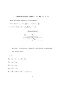
DERIVATION OF MOSFET I VS. V C GS V - UMD
user.eng.umd.eduDERIVATION OF MOSFET I DS VS. V DS + V GS 3 I D= J nW(W=Device Width) J n for channel is Amp/cm since Q m= Charge=cm2 I D for Linear Region: I D= C ox W L [(V GS V TH)V DS V2 DS 2] 2. Saturation Region When V DS (V GS V TH) channel pinches o .This means that the channel current near the drain spreads out and the channel near drain can be approximated

N-Channel 20 V (D-S) MOSFET - Vishay Intertechnology
www.vishay.comVishay Siliconix Package Information Document Number: 71196 09-Jul-01 www.vishay.com 1 SOT-23 (TO-236): 3-LEAD b 1E 1 3 2 S e e1 D A 2 A1 C Seating Plane 0.10 mm 0.004"
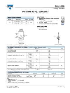
P-Channel 40 V (D-S) MOSFET - Vishay Intertechnology
www.vishay.comP-Channel 40 V (D-S) MOSFET FEATURES • Halogen-free According to IEC 61249-2-21 Definition TEFhcne †Tr ® Power MOSFET † 100 % Rg Tested † Compliant to RoHS Directive 2002/95/EC APPLICATIONS † Load Switch † DC/DC Converter Notes: a. Based on TC = 25 °C. b. Surface mounted on 1" x 1" FR4 board. c. t = 5 s. d.

LTC4441/LTC4441-1 - N-Channel MOSFET Gate Driver
www.analog.comLTC4441/LTC4441-1 1 44411fa Typical applicaTion FeaTures DescripTion N-Channel MOSFET Gate Driver The LTC®4441/LTC4441-1 is an N-channel MOSFET gate driver that can supply up to 6A of peak output current.

Document information AN11158 - Nexperia
assets.nexperia.comUnderstanding power MOSFET data sheet parameters 2.2. Pinning information This section describes the internal connections and general layout of the device. Note that the symbol is for an enhancement mode n-channel MOSFET with the source and body tied together, and a parallel diode between the source and drain. The parallel diode is known as the ...
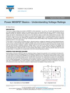
Power MOSFET Basics - Understanding Voltage Ratings
www.mouser.comPower MOSFET Basics - Understanding Voltage Ratings www.vishay.com Revision: 12-Jan-17 1 Document Number: 75079 ... Power MOSFET Basics - Understanding Voltage Ratings Application Note AN851 www.vishay.com Vishay Siliconix APPLICATION NOTE Revision: 12-Jan-17 2 Document Number: 75079

NVMFS5C460NL MOSFET – Power, Single N-Channel
www.onsemi.com3. Maximum current for pulses as long as 1 second is higher but is dependent on pulse duration and duty cycle. MARKING www.onsemi.com XXXXXX AYWZZ G (4) S (1,2,3) N−CHANNEL MOSFET D (5,6) S S S G D D D D DFN5 (SO−8FL) CASE 488AA STYLE 1 1 See detailed ordering, marking and shipping information in the package dimensions section on page 5 of ...

4.3 MOSFET Circuits at DC - ITTC
www.ittc.ku.eduMOSFET Circuits To analyze MOSFET circuit with D.C. sources, we must follow these five steps: 1. ASSUME an operating mode 2. ENFORCE the equality conditions of that mode. 3. ANALYZE the circuit with the enforced conditions. 4. CHECK the inequality conditions of the mode for consistency with original assumption. If consistent, the
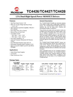
TC4426/TC4427/TC4428 1.5A Dual High-Speed Power …
ww1.microchip.comMar 25, 2014 · MOSFET’s intended state is not affected, even by large transients. Other compatible drivers are the TC4426A/TC4427A/ TC4428A family of devices. The TC4426A/TC4427A/ TC4428A devices have matched leading and falling ... CHARACTERISTICS Absolute Maximum Ratings † ...

P-Channel 60-V (D-S) MOSFET - Vishay Intertechnology
www.vishay.comOrdering Information: Si2309CDS-T1-E3 (Lead (Pb)-free) Si2309CDS-T1-GE3 (Lead (Pb)-free and Halogen-free) G TO-236 (SOT-23) S D Top View 2 3 1 * Marking Code ... not subject to production testing. ... rating conditions for extended periods may affect device reliability. SPECIFICATIONS TJ = 25 °C, unless otherwise noted
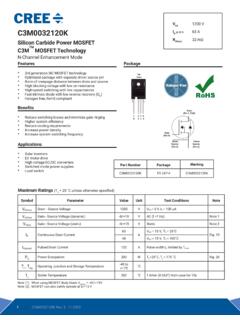
VDS C3M0032120K I D R 32 mΩ
assets.wolfspeed.com1 C3M0032120K Rev. - 06-2019 C3M0032120K Silicon Carbide Power MOSFET C3M TM MOSFET Technology N-Channel Enhancement Mode Features • 3rd generation SiC MOSFET technology • Optimized package with separate driver source pin • 8mm of creepage distance between drain and source • High blocking voltage with low on-resistance • High-speed …

NCP302155 - Integrated Driver and MOSFET
www.onsemi.comThe NCP302155 integrates a MOSFET driver, high−side MOSFET ... 27, 33 GL Low Side FET Gate Access (pin 27 and pad 33 are internally connected) 29 VCCD Driver Power Supply Input ... Input Voltage High VPWM_HI 2.65 − − V Input Mid−state Voltage VPWM_MID 1.4 − 2.1 V

富士パワーMOSFET - 富士電機
www.fujielectric.co.jp図1-4にこれまで開発した当社パワーMOSFET の系列を示します。 高耐圧Power MOSFET 低耐圧PowerMOSFET 1980 1990 1995 2000 2010 図1-4.富士パワーMOSFET 系列表 SIPMOS (F-0) F-Ⅰ F-Ⅱ FAP-Ⅱ FAP-ⅡA FAP-ⅡS series SuperFAP-G series SuperFAP-E3 series Super Junction MOSFET F-Ⅰ F-Ⅲ FAP-Ⅲ FAP-ⅢA

Super Junction MOSFET LLC コンバータの1次側スイッチン …
fscdn.rohm.comSuper Junction MOSFET シリーズ LLC コンバータの1次側スイッチング素子における PrestoMOSTM の有用性について LLC コンバータはインダクタL と容量C の共振を利用することによって、トランスの1 次側のスイッチング素子のターンON 時にゼロ電圧スイッチン

MOSFETの破壊メカニズムについて - fscdn.rohm.com
fscdn.rohm.comMOSFETを安全に使用するには、このSOA範囲内で使用 する必要があり、この範囲を超えると破壊に至る可能性があります。このSOAの範囲外で動作させた場合の破壊をSOA破壊と呼んでいます。例 として、弊社SJ-MOS(Super Junction MOSFET) R6024KNXのSOAを図1に示します。 …
窒化物半導体の特徴とデバイス展開
www.rciqe.hokudai.ac.jpサファイア, Si, SiC AlGaN 2次元電子層 i-GaN AlGaN GaN S G D HEMT: High Electron Mobility Transistor 1 x 10¹³ 1 x 10¹² キャリア密度 (cm-2) SiC MOSFET 2000 GaN HEMT 100-500 チャネル移動度 (cm2/Vs) 基板がない -> 基板を選ばない ½
LLC Resonant Converter for Battery Charging Application
irphouse.comThe power factor correction stage is a continuous conduction mode of boost topology. ... Before turning ON the MOSFET switch the voltage across the switch should be equal to zero. When the switch S1is ON, the resonant current starts to increase across the inductor Lr. The magnetizing inductance which is coupled to the load side
TEORI DASAR MOSFET - Universitas Brawijaya
maulana.lecture.ub.ac.idGambar 1 Simbol Transistor MOSFET Mode Depletion (a). N-Channel Depletion (b). P-Channel Depletion 2) Transistor Mode peningkatan (Transistor Mode Enhancement) Transistor mode enhancement ini pada fisiknya tidak memiliki saluran antara drain dan sourcenya karena lapisan bulk meluas dengan lapisan SiO ...
Similar queries
Power MOSFETs, IXYS, Switch MOSFETs, MOSFETs, Applications, Depletion, Mode, Mode MOSFET, Depletion-mode MOSFET, Power MOSFET Basics: Understanding Gate Charge and, Vishay, Power MOSFET, Vishay Intertechnology, Power, Switching, LTC1144, Switch, APPLICATION, Channel, MOSFET, MOSFET transistor I-V characteristics, Power MOSFET Basics Understanding Superjunction, Rated, Resistance, Super, Junction, Sic-mosfet, Sic -mosfet, SiC MOSFET, Silicon carbide MOSFET, Synchronous, Parameters, Voltage, Design Guide for QR Flyback Converter, Mouser Electronics, Power factor correction, IGBT/MOSFET Gate Drive Optocoupler, Drive, Inverter, Models, High voltage, Technology, Single, Channel MOSFET, DERIVATION OF MOSFET I, N-Channel, Power MOSFET Basics - Understanding Voltage Ratings, NVMFS5C460NL MOSFET – Power, Single N-Channel, Pulses, CHARACTERISTICS, P-Channel 60-V (D-S) MOSFET, Lead, Free, Testing, Reliability, Silicon Carbide, NCP302155 - Integrated Driver and MOSFET, High, Voltage High, Super Junction MOSFET, Super Junction MOSFET LLC, MOSFET Mode Depletion