Search results with tag "Junction"

Bipolar Junction Transistor (BJT) Basics- GATE Problems
www.gatestudy.com(a) Bipolar junction transistors (b) NMOS transistors (c) Unipolar junction transistors (d) Junction field – effect transistors [GATE 1995] Soln. Ebers Moll model is one of classical models of BJT for small signals. This model is based on interacting diode junctions and is applicable to any transistor operating modes Option (a)

Lecture 9: PN Junctions - University of California, Berkeley
inst.eecs.berkeley.eduDepartment of EECS University of California, Berkeley EECS 105Fall 2003, Lecture 9 Prof. A. Niknejad n-type p-type ND NA PN Junctions: Overview The most important device is a junction between a p-type region and an n-type region When the junction is first formed, due to the concentration gradient, mobile charges transfer near junction

Store Store Address - Boots
www.boots.comCREWE GRAND JUNCTION RP Unit 12 Grand Junction Retail Park Grand Junction Way CREWE Cheshire CW12RP Croydon Whitgift Centre 12-18 Whitgift Centre The Mall CROYDON Surrey CR91SN ... YEOVIL MIDDLE ST 37 Middle Street YEOVIL Somerset BA201LS . Author: Georgia Richardson

W-Series Junction Boxes
www.crouse-hindslatam.comW-Series Boxes WJBF Checkered Cover Sidewalk Junction Boxes Heavy Duty External Flanged for Flush Mounting Applications: WJBF boxes are primarily designed for surface mounting. WJBF heavy duty junction boxes are installed in conduit systems to: • Act as pull box for conductors • Provide openings and space for making splices and taps in ...
International Transistor Equivalents Guide
worldradiohistory.comC complementary transistor NPN/PNP DG dual germanium transistor DJ dual junction transistor DS dual silicon transistor FET field effect transistor G germanium transistor GD germanium Darlington transistor J junction FET (JFET) M MOSFET ME multiple -emitter transistor MOS metal oxide semiconductor P photo -transistor PU programmable unijunction ...
Lecture 13: Amplifier Noise Calculations
rfic.eecs.berkeley.eduFET Layout To reduce the gate resistance, a multi-finger layout approach is commonly adopted. As a bonus, the junction capacitance is reduced due to the junction sharing. A. M. Niknejad University of California, Berkeley EECS 142 Lecture 13 p. 10/20 – p

PN Junction Diode: I-V Characteristics
ocw.snu.ac.krChapter 6. PN Junction Diode : I-V Characteristics üWhenever an electron on the p-side moves to the n-side, it is replaced by an electron generated through one of the R-G centers ohmic ohmic minority minority excess majority carriers àlocal excess majority carriers àlocal E E Excess carriers move to the contact with a relaxation time ...

2N3904/MMBT3904/PZT3904 NPN General Purpose Amplifier
www.farnell.comRθJC Thermal Resistance, Junction to Case 83.3 °C/W RθJA Thermal Resistance, Junction to Ambient 200 357 125 °C/W * Device mounted on FR-4 PCB 1.6" X 1.6" X 0.06." ** Device mounted on FR-4 PCB 36 mm X 18 mm X 1.5 mm; mounting pad for the collector lead min. 6 cm 2. 2N3904 MMBT3904 SOT-23 Mark: 1A PZT3904 2N3904 / MMBT3904 / PZT3904

Super Junction MOSFET LLC コンバータの1次側スイッチン …
fscdn.rohm.comSuper Junction MOSFET シリーズ LLC コンバータの1次側スイッチング素子における PrestoMOSTM の有用性について LLC コンバータはインダクタL と容量C の共振を利用することによって、トランスの1 次側のスイッチング素子のターンON 時にゼロ電圧スイッチン

MPDB Series - MERSEN
ep-us.mersen.comMersen power distribution blocks provide a safe and easy method of splicing cables, splitting primary power into secondary circuits and fulfilling requirements for fixed junction tap-off points. Unless noted otherwise, all blocks are UL and CSA approved while meeting spacing requirements for feeder and branch circuits in conjunction with

Closure of the M42 motorway between junctions 9 and 10
assets.hs2.org.ukbetween junctions 9 and 10 Friday 24 December to Friday 31 December 2021 October 2021 | www.hs2.org.uk High Speed Two (HS2) is the new high speed railway for Britain. Balfour Beatty VINCI is working in partnership with HS2 Ltd to build the new high speed railway in your area.

Chapter 2 Semiconductor Heterostructures - Cornell …
courses.cit.cornell.eduexactly zero in the depletion regions of thicknesses xp and xn on the p-side and n-side of the junction, respectively. It is a good approximation to calculate the junction electric field and potential. The net charge density in the depletion regions is then due to the ionized donors and acceptors and is as shown below.

How to Implement a MOSFET with a Gate Driver
www.egr.msu.eduNov 13, 2014 · Frequency, Junction. Introduction A MOSFET is an acronym for metal-oxide semiconductor field-effect transistor. It is a special type of field-effect transistor (FET) and is the key component in high frequency, high efficiency switching applications across the electronics industry. A MOSFET is a voltage controlled device.

Terminal Junction Systems MIL-T-81714 Series I Class D
www.amphenol.co.jpwww.amphenolpcd.com Milaero@amphenolpcd.com 1-978-624-3400 72 Cherry Hill Drive Beverly, MA 01915 M81714/2, /7 Series I Size 20 Class D Materials Module Body: Polyetherimide per ASTM-D5205 Grommet: Silicone Blend Elastomer per A-A-59588 Contact Retainers: Stainless steel Socket Contacts:

Metal/Semiconductor Ohmic Contacts - Stanford University
web.stanford.edu1 components of the resistance associated with the S/D junctions of a MOS transistor. Rcsd will be a dominant component for highly scaled nanometer transistor (Rcsd/Rseries ↑ >> ~ 60 % for LG < 53 nm) 32 nm53 nm70 nm100 nm 0 10 20 30 40 50 60 70 R dp R ext R ov R NMOS csd Physical Gate Length Relative Contribution [%] 30 nm50 nm70 nm100 nm 0 ...

WIRING DIAGRAMS - 73-87ChevyTrucks.com
www.73-87chevytrucks.commore practical to use a single wire protected by a braided tubing called a loom. Wiring harnesses are joined by using a multiple plug and receptacle connector block, or a terminal post chassis junction block. In the instrument panel area plastic insulated blade-type connectors and screw-type terminals are used.

TFL Base Map
content.tfl.gov.ukClapham Peckham Penge BeckenhamBromley Orpington Croydon Purley Carshalton Wallington Richmond Northwood Harefield Hounslow Harrow East Barnet Finchley Hendon Hampstead Paddington ... Motorway with junction A road Railway/Tram line Greater London boundary London borough boundaries Woodland and Parkland Rivers and lakes TfL North & West area

Single-gang - Eaton
www.eaton.comWeatherproof outlet boxes Applications: • For use as a weatherproof junction box, device housing or as a lampholder mounting in damp or wet locations Standard materials: • Boxes – die cast aluminum • Gaskets – polyethylene foam 4” ROUND – 1-1/ 2” DEEP A Cat. # Outlet holes Cubic inches Color Unit qty. Wt.

Appendix 2 - Street Mail Service Conditions of Delivery
auspost.com.auboxes at the junction of the main thoroughfare and the driveway or walkway. The same applies if access to a number of premises from the main thoroughfare is restricted. If the development does not meet all the conditions, delivery is to either: a group of mail boxes at the boundary of the private road with a public ro ad, or

Freedom Pass Map - National Rail
www.nationalrail.co.ukClapham Junction City Thameslink CHARING CROSS Tottenham Court Road Oxford Circus Green Park VICTORIA WATERLOO Vauxhall Farringdon Old Street Moorgate KING’S CROSS Highbury & Islington Finsbury Park Bank CANNON STREET Elephant & Castle LIVERPOOL STREET FENCHURCH STREET Tower Hill LONDON BRIDGE New Cross New Cross Gate …

ON Semiconductor Is Now
www.onsemi.comapplication compare among regular, super junction MOSFET and even IGBT devices is feasible, while still using the same setup. It is important to mention that insulation barrier between primary and secondary side at MOSFET drivers level is provided …

Electrical Inspection Checklists
samples.jbpub.com11. Check for adequate length of free conductors in boxes. 300.14 12. Verify that boxes are installed at junction, splice, outlet, switch, and pull points. 300.15 13. Check conductor fill in raceways. 300.17 14. Verify that raceway systems are complete prior to installation of conductors. 300.18(A) 15. Check vertical raceways for adequate ...

Power MOSFET Basics - Tayloredge
www.tayloredge.comtransistor (MOSFET) is based on the original field-effect transistor introduced in the 70s. Figure 1 shows the device schematic, transfer characteristics and device symbol for a MOSFET. The invention of the power MOSFET was partly driven by the limitations of bipolar power junction transistors (BJTs) which, until recently, was the device of ...

DEPARTMENT OF ENVIRONMENTAL PROTECTION Bureau of ...
www1.nyc.gov59-17 Junction Boulevard, 9. th: Floor, Flushing, New York 11373 . Records Control (718) 595–3855. CONSTRUCTION NOISE MITIGATION PLAN. Construction Noise Mitigation Plan Rev 04/2019 . MUST PRINT AND POST ON WORKSITE.

MARKET DATE OF TYPE OF PROPERTY ADDRESS PARISH …
www.jncb.comLongville Boulevard in the residential subdivision and housing development of Longville Park, which is located ... over a bridge until reaching a junction and then making a left turn onto a parochial road. The subject property ... Clarendon 1256/785 $10M 17-Oct-14 Residential Available Two storey residence with ground floor - kitchen,living ...

SRT2 EDGE-LIT
hubbellcdn.com701 Millennium Boulevard • Greenville, SC 29607 / Tel 864.678.1000 / Website www.beaconproducts.com FEATURES ... square junction box or octagonal box and ... 5C 5684 118.17 2 0 2 5657 117.60 2 0 2 5439 113.08 2 0 2

Bipolar Transistor - Chenming Hu
www.chu.berkeley.edubipolar transistor models are introduced, i.e. , Ebers–Moll model, small-signal model, and charge control model. Each model has its own areas of applications. he bipolar junction transistor or BJT was invented in 1948 at Bell Telephone Laboratories, New Jersey, USA. It was the first mass produced transistor,

EPC2019 – Enhancement Mode Power Transistor
epc-co.comeGaN® FET DATASHEET EPC2019 EPC – POWER CONVERSION TECHNOLOGY LEADER | EPC-CO.COM | ©2022 | | 4 Figure 12: Transient Thermal Response Curves Junction-to-Board t1, Rectangular Pulse Duration, seconds Duty Cycle: Notes: Duty Factor: D = t 1/t 2 Peak T J = P DM x Z θJB x R θJB + T B P DM t 1 t 2 0.5 0.1 0.05 0.02 0.01 Z Single Pulse θJB
MOSFET Device Physics and Operation
homepages.rpi.eduthe mobile charge in the channel by capacitive coupling (field effect). Examples of FETs based on these principles are metal-oxide-semiconductor FET (MOSFET), junction FET (JFET), metal-semiconductor FET (MESFET), and heterostructure FET (HFETs). In all cases, the stationary gate-channel impedance is very large at normal operating conditions.

Surface-Mount TRANSZORB Transient Voltage Suppressors
www.vishay.com• Glass passivated chip junction • Available in unidirectional and bidirectional • 400 W peak pulse power capability with a 10/1000 μs waveform, repetitive rate (duty cycle): 0.01 % (300 W above 91 V) • Excellent clamping capability • Very fast response time • …
150V VIN and VOUT Synchronous 4-Switch Buck-Boost ...
www.analog.comLT 3779 4 For more information www.analog.com ELECTRICAL CHARACTERISTICS The l denotes the specifications which apply over the specified operating junction temperature range, otherwise specifications are at TA = 25°C (Note 2), VIN = 15V, VRUN = 5V, VEXTVCC = 0V, VDRVSET = 0V, VVINOV = 0V unless otherwise noted. SYMBOL PARAMETER CONDITIONS …

CHAPTER 6. TREATMENT OF SPECIFIC AVIONICS EQUIPMENT
www.faa.govchapter 4, paragraph 407. c. Engine Compartments. Inspect compartment hardware, electrical wire bundles and connectors, terminal boards, and junction boxes for evidence of corrosion and damage (Figure 6-1). (1) Repair or replace damaged components as required. (2) Clean and treat corrosion in accordance with paragraphs 602b(2) through (6) with the

Agent Name Address Contact number - Singapore Air
www.singaporeair.com#01-05 Pioneer Junction Singapore 627066 6710 4933 SHILLA TRAVEL RETAIL PTE LTD 30 Pasir Panjang Road Level 15 Mapletree Business City Singapore 117440 6833 1663 ... SUPER TRAVELS PTE LTD 133 New Bridge Road #03-01/02, Chinatown Point Singapore 059413 6392 3688. Agent Name Address Contact number TEN GROUP SINGAPORE PTE LTD

富士パワーMOSFET - 富士電機
www.fujielectric.co.jp図1-4にこれまで開発した当社パワーMOSFET の系列を示します。 高耐圧Power MOSFET 低耐圧PowerMOSFET 1980 1990 1995 2000 2010 図1-4.富士パワーMOSFET 系列表 SIPMOS (F-0) F-Ⅰ F-Ⅱ FAP-Ⅱ FAP-ⅡA FAP-ⅡS series SuperFAP-G series SuperFAP-E3 series Super Junction MOSFET F-Ⅰ F-Ⅲ FAP-Ⅲ FAP-ⅢA

MOSFETの破壊メカニズムについて - fscdn.rohm.com
fscdn.rohm.comMOSFETを安全に使用するには、このSOA範囲内で使用 する必要があり、この範囲を超えると破壊に至る可能性があります。このSOAの範囲外で動作させた場合の破壊をSOA破壊と呼んでいます。例 として、弊社SJ-MOS(Super Junction MOSFET) R6024KNXのSOAを図1に示します。 …

GAN POWER TRANSISTORS - Panasonic
eu.industrial.panasonic.comcon-based super-junction MOSFETs (see Figure 3). The Figure-of-Merit (RDS(on) ∙ QG) of a 600V/70nOhm GiT is value of modern silicon components. GATE DRIVING PRINCIPLE The GiT transistor is controlled as mix of a field effect transis-tor and (bi)polar transistor. As with FETs, a positive threshold

パワーモジュールの最新動向と展望
www.giho.mitsubishielectric.co.jpが,図2に示すようにJFET(Junction Field Effect Tran - sistor)長が一定以下になると急激にオン抵抗が上昇する。 当社の第2世代SiC MOSFETではこの問題を解決するた めにJFET部の濃度プロファイルを最適化させて高性能化 を実現している。

HID Signo Reader Installation Guide - hidglobal.com
www.hidglobal.comscrews (2) – for Metric (EU etc) junction box installation Flat head/countersunk 0.138-32 x 0.375" security screw (1) – alternative anti-tamper screw for attaching the reader to the mounting plate 5-pin terminal connectors, terminal strip models only (2) Recommended parts (not supplied) Cable, 5-10 conductor (Wiegand or
C TABLE 9 Type K Thermocouple thermoelectric voltage as a ...
www.pyromation.comTABLE 9 Type K Thermocouple thermoelectric voltage as a function of temperature (°C); reference junctions at 0 °C °C 0 1 2 3 4 5 6 7 8 9 10 °C Thermoelectric ...

SSE/Dev CDE/Elec - Integral Coach Factory
icf.indianrailways.gov.in(new) or wp (old) of table-2 of is: 1285 16 31 b38 terminal strip assembly 17 32 b39 roof through box to drg no.emu/dmc/ac/76011,mcb boxes to is: 8623,all junction boxes 18 33 b40 modular integrated pantry unit for buffet coaches to rcf spec. no..edts 118 for lhb 19 34 b41 composite pantry for chair car/ecc/ accn/ accw to rcf spec no.

Power MOSFET Selection Guide - NXP
www.nxp.comA MOSFET’s RDSon is given by the formula: RDSon = Rchannel + Rdrift + Rsubstrate + (Rpackage) Many manufacturers focus on reducing Rchannel to drive RDSon down. NXP’s Super-junction allows for an optimisation of all 3 components for reduction in RDSon, whilst also enhancing switching performance and Safe Operating Area. Maximising Switching ...
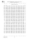
BSS84 - P-Channel Enhancement Mode Field-Effect Transistor
www.onsemi.comThis P−channel enhancement−mode field−effect transistor is produced using onsemi’s proprietary, high cell density, DMOS technology. This very high density process minimizes on−state ... R JA is the sum of the junction−to−case and case−to−ambient thermal resistance where the case thermal reference is defined as the solder

Band-bending - Iowa State University
tuttle.merc.iastate.eduIn the p-n junction and BJT, we saw that the semiconductor band edges were bent in the depletion layers. We used the depletion approximation and Poisson’s equation to relate the band-bending (barrier height) to the electric field to the depletion layer width. In the case of depletion, our treatment is reasonably accurate. However, we

SN74LVC1G3157 Single-Pole Double-Throw Analog Switch ...
www.ti.comTJ Junction temperature 150 °C Tstg Storage temperature –65 150 °C (1) JEDEC document JEP155 states that 500-V HBM allows safe manufacturing with a standard ESD control process. (2) JEDEC document JEP157 states that 250-V CDM allows safe manufacturing with a standard ESD control process. 6.2 ESD Ratings VALUE UNIT V(ESD) Electrostatic discharge

Steel City Metallic Boxes & Covers - USESI Careers
www.usesi.com2" & 3⁄ 4" Knockout Pryouts Cable Pryouts Always in Pairs 21 ... Device, and Junction Boxes, and Conduit Bodies. Boxes and conduit bodies shall be of sufficient size to provide free space for all enclosed conductors. In no case shall the volume of the box, as ... of motor or generator terminal housings, see Article 430.12. Boxes and

Design of Flexible-Duct Junction Boxes - Energy
www.energy.govACCA Manual D, Group 11 Fittings • Recommendations: • Entrance has a diffuse fitting that recovers velocity pressures and prevents swirl (optional) • Straight approach and straight exit • Exit opening on side (no top or bottom exits) • Exit opening at least two diameters from entrance (L) • Make box as small as possible, but comply with
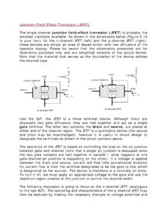
Junction Field Effect Transistor (JFET)
coefs.uncc.eduJunction Field Effect Transistor (JFET) The single channel junction field-effect transistor (JFET) is probably the simplest transistor available. As shown in the schematics below (Figure 6.13 in your text) for the n-channel JFET (left) and the p-channel JFET (right), these devices are simply an area of doped silicon with two diffusions of the
Similar queries
Bipolar Junction Transistor (BJT) Basics- GATE Problems, Junction, Junction field – effect, Lecture 9: PN Junctions, Berkeley, Store Store Address, YEOVIL, Junction Boxes, Boxes WJBF Checkered Cover Sidewalk Junction Boxes, WJBF boxes, WJBF, Transistor, Junction transistor, Field effect transistor, Junction FET, JFET, Noise, PN Junction, NPN General Purpose Amplifier, Super Junction MOSFET LLC, Super Junction MOSFET, MPDB, Blocks, Junctions, Chapter 2 Semiconductor Heterostructures, Field, Effect, Terminal Junction Systems MIL-T-81714 Series, 3400, Series, WIRING DIAGRAMS, Single, Terminal, Clapham, Eaton, Boxes, National Rail, Clapham Junction, MOSFET, Splice, Pull, Power MOSFET Basics, 17 Junction Boulevard, Boulevard, SRT2 EDGE-LIT, Models, Bipolar junction transistor, EPC2019 – Enhancement Mode Power Transistor, Channel, Glass passivated, Fast, Singapore Air, Super, Junction Field Effect Tran - sistor, Band-bending, Design of Flexible-Duct Junction Boxes, ACCA, Junction Field Effect Transistor JFET, Junction field-effect transistor JFET