Search results with tag "Jfet"
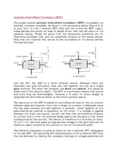
Junction Field Effect Transistor (JFET)
coefs.uncc.eduJunction Field Effect Transistor (JFET) The single channel junction field-effect transistor (JFET) is probably the simplest transistor available. As shown in the schematics below (Figure 6.13 in your text) for the n-channel JFET (left) and the p-channel JFET (right), these devices are simply an area of doped silicon with two diffusions of the

LT1057/LT1058 - Dual and Quad, JFET Input Precision High ...
www.analog.comJFET input duals. The LT1058 is the lowest offset quad JFET input operational amplifier in the standard 14-pin configuration. It offers significant accuracy improvement over presently available JFET input quad operational amplifiers. The LT1058 can replace four single precision JFET input op amps, while saving board space, power dissipation and ...
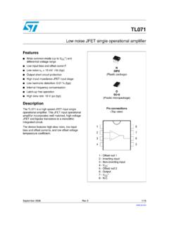
Low noise JFET single operational amplifier
www.st.comSep 19, 2008 · The TL071 is a high-speed JFET input single operational amplifier. This JFET input operational amplifier incorporates well matched, high-voltage JFET and bipolar transistors in a monolithic integrated circuit. The device features high slew rates, low input bias and offset currents, and low offset voltage temperature coefficient. N DIP8 (Plastic ...
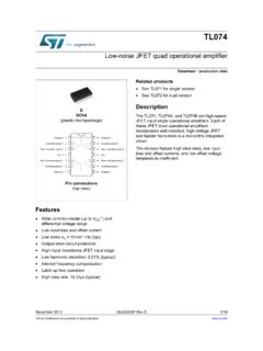
Low-noise JFET quad operational amplifier
www.st.comJul 07, 2008 · JFET input single operational amplifiers. Each of these JFET input operational amplifiers incorporates well matched, high-voltage JFET and bipolar transistors in a monolithic integrated circuit. The devices feature high slew rates, low input bias and offset currents, and low offset voltage temperature coefficient. Inverting Input 2 Non ...
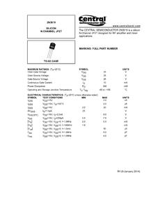
2N3819 SILICON N-CHANNEL JFET N-Channel JFET designed …
my.centralsemi.comN-CHANNEL JFET The CENTRAL SEMICONDUCTOR 2N3819 is a silicon N-Channel JFET designed for RF amplifier and mixer applications. MARKING: FULL PART NUMBER MAXIMUM RATINGS: (TA=25°C) SYMBOL UNITS Drain-Gate Voltage VDG 25 V Drain-Source Voltage VDS 25 V Gate-Source Voltage VGS 25 V Continuous Gate Current IG 10 mA Power Dissipation …

Field Effect Transistors - Learn About Electronics
learnabout-electronics.orgJFET Circuit Symbols P channel JFETs are also available and the principle of operation is the same as the N channel type described here, but polarities of the voltages are of course reversed, and the charge carriers are holes. Notice in the JFET circuit symbols shown in Fig.

LF353-NWide Bandwidth Dual JFET Input Operational Amplifier
www.ti.comLF353-NWide Bandwidth Dual JFET Input Operational Amplifier Check for Samples: LF353-N 1FEATURES DESCRIPTION These devices are low cost, high speed, dual JFET 2• Internally Trimmed Offset Voltage: 10 mV input operational amplifiers with an internally trimmed • Low Input Bias Current: 50pA input offset voltage (BI-FET II technology). They
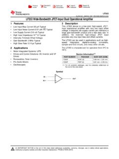
LF353 Wide-Bandwidth JFET-Input Dual Operational …
www.ti.comThe LF353 device is a JFET-input operational amplifier with low input bias and offset currents and fast slew rate. Each amplifier features JFET inputs (for high input impedance) coupled with bipolar output stages integrated on a single monolithic chip. The output is protected against shorts due to the resistive 200-Ωoutput impedance.
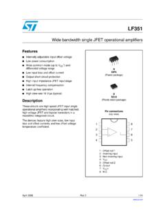
Wide bandwidth single JFET operational amplifiers
www.st.comApril 2008 Rev 2 1/14 14 LF351 Wide bandwidth single JFET operational amplifiers Features Internally adjustable input offset voltage Low power consumption Wide common-mode (up to VCC +) and differential voltage range Low input bias and offset current Output short-circuit protection High input impedance JFET input stage Internal frequency compensation

General purpose JFET single operational amplifiers
www.st.comJun 27, 2008 · JFET input single operational amplifiers incorporating well matched, high-voltage JFET and bipolar transistors in a monolithic integrated circuit. The devices feature high slew rates, low input bias and offset currents, and low offset voltage temperature coefficient. N DIP8 (Plastic package) D SO-8 (Plastic micropackage) 1 - Offset null 1
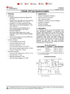
LF356-MIL JFET Input Operational Amplifier datasheet
www.ti.com• Logarithmic Amplifiers • Photocell Amplifiers • Sample and Hold Circuits 3 Description The LF356-MIL device are the first monolithic JFET input operational amplifiers to incorporate well-matched, high-voltage JFETs on the same chip with standard bipolar transistors (BI-FET™ Technology). These amplifiers feature low input bias and offset
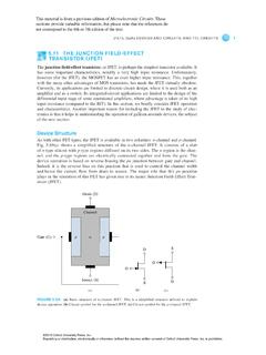
5.11 THE JUNCTION FIELD-EFFECT TRANSISTOR (JFET)
global.oup.comin the enhancement mode (by simply applying a positive v GS if the device is n channel) this is impossible in the JFET case. If we attempt to apply a positive v GS, the gate–channel pn junction becomes forward biased and the gate ceases to control the channel. Thus the maximum v GS
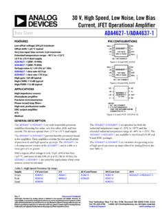
30 V, High Speed, Low Noise, Low Bias Current, JFET ...
www.analog.com30 V, High Speed, Low Noise, Low Bias Current, JFET Operational Amplifier Data Sheet ADA4627-1/ADA4637-1 Rev. F Document Feedback Information furnished by Analog Devices is believed to be accurate and reliable. However, no responsibility is assumed by Analog Devices for its use, nor for any infringements of patents or other

Dual Bipolar/JFET, Audio Operational Amplifier OP275
www.analog.comHigh Performance Audio Active Filters. Fast Amplifiers Integrators. PIN CONNECTIONS GENERAL DESCRIPTION. The OP275 is the first amplifier to feature the Butler Amplifier front end. This new front end design combines both bipolar . and JFET transistors to attain amplifiers with the accuracy and low noise performance of bipolar transistors, and ...
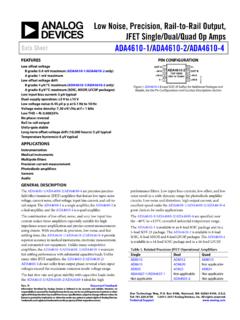
Low Noise, Precision, Rail-to-Rail Output, JFET Single ...
www.analog.comADA4610-1/ADA4610-2/ADA4610-4 are precision junction field effect transistor (JFET) amplifiers that feature low input noise voltage, current noise, offset voltage, input bias current, and rail -to-rail output. The ADA4610-1 is a single amplifier , the ADA4610-2 is a dual amplifier, and the ADA4610-4 is a quad amplifier.
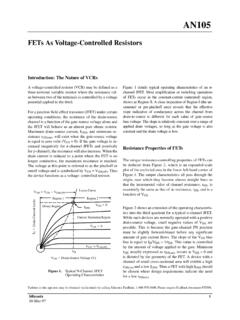
Introduction: The Nature of VCRs
www.vishay.comFor a junction field-effect transistor (JFET) under certain operating conditions, the resistance of the drain-source channel is a function of the gate-source voltage alone and the JFET will behave as an almost pure ohmic resistor. Maximum drain-source current, I DSS, and minimum re-sistance rDS(on), will exist when the gate-source voltage
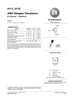
J111, J112 - JFET Chopper Transistors
www.onsemi.comJFET Chopper Transistors N−Channel — Depletion Features • Pb−Free Packages are Available* MAXIMUM RATINGS Rating Symbol Value Unit Drain−Gate Voltage VDG −35 Vdc Gate−Source Voltage VGS −35 Vdc Gate Current IG 50 mAdc Total Device Dissipation @ TA = 25°C Derate above = 25°C PD 350 2.8 mW mW/°C Lead Temperature TL 300 °C ...
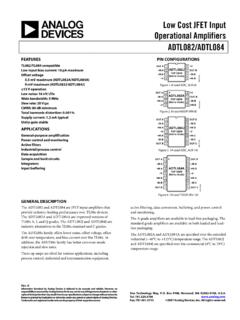
ADTL082/ADTL084 Low Cost JFET Input Operational …
www.analog.comLow Cost JFET Input Operational Amplifiers ADTL082/ADTL084 Rev. B Information furnished by Analog Devices is believed to be accurate and reliable. However, no responsibility is assumed by Analog Devices for its use, nor for any infringements of patents or other rights of third parties that may result from its use.

AD8610/AD8620 Precision, Very Low Noise, Low Input Bias ...
www.analog.comThe AD8610/AD8620 are very high precision JFET input ampli- fiers featuring ultralow offset voltage and drift, very low input voltage and current noise, very low input bias current, and wide bandwidth. Unlike many JFET amplifiers, the AD8610/AD8620 input bias current is low over the entire operating temperature range.
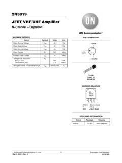
2N3819 JFET VHF/UHF Amplifier - ON Semiconductor
www.onsemi.comSemiconductor Components Industries, LLC, 2002 March, 2002 – Rev. 0 1 Publication Order Number: 2N3819/D 2N3819 JFET VHF/UHF Amplifier N–Channel – Depletion
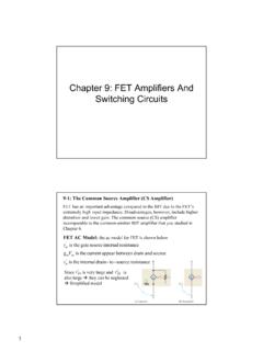
Chapter 9: FET Amplifiers And Switching Circuits
staff-old.najah.eduThe ac analysis is the same as for the JFET amplifier. 9-1: The Common Source Amplifier E-MOSFET Amplifier Operation: A voltage divider common-source amplifier for n-channel E-MOSFET is shown. The gate is biased with a positive voltage such that VGS > VGS(th) Dc analysis Ac analysis where Voltage gain is same as for JFET m d gs ds in out v g R ...

第7回半導体工学 20171120 - 名古屋大学
www.echo.nuee.nagoya-u.ac.jp接合型(jfet) sd g g n ゲートに逆バイアスをかける。 →空乏層が拡がる。 jfetの動作原理 電子の流れを空乏層 幅で調整 空乏層 チャネルと呼ぶ p p 35/80
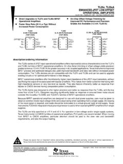
TL05x, TL05xA ENHANCED-JFET LOW-OFFSET OPERATIONAL …
www.ti.comTL05x, TL05xA ENHANCED-JFET LOW-OFFSET OPERATIONAL AMPLIFIERS SLOS178A – FEBRUARY 1997 - REVISED FEBRUARY 2003 4 POST OFFICE BOX 655303 • DALLAS, TEXAS 75265 absolute maximum ratings over operating free-air temperature range (unless otherwise noted)†
LF147/LF347 Wide Bandwidth Quad JFET Input Operational ...
www.ti.comLF147, LF347-N www.ti.com SNOSBH1D – MAY 1999– REVISED MARCH 2013 LF147/LF347 Wide Bandwidth Quad JFET Input Operational Amplifiers Check for Samples: LF147, LF347-N
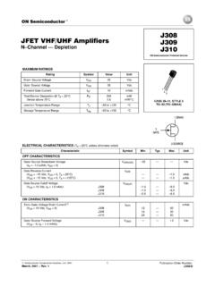
J308 JFET VHF/UHF Amplifiers J309 N–Channel — …
www.g1sle.comJFET VHF/UHF Amplifiers N–Channel — Depletion MAXIMUM RATINGS Rating Symbol Value Unit Drain–Source Voltage VDS 25 Vdc Gate–Source Voltage VGS 25 Vdc Forward Gate Current IGF 10 mAdc
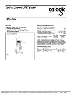
Dual N-Channel JFET Switch
www.calogic.netelectrical characteristics (t. a = 25. o. c unless otherwise specified) symbol parameter u401 u402 u403 u404 u405 u406 units test conditions min max min max min max min max min max min max
TL082 Wide Bandwidth Dual JFET Input Operational …
www.ti.comAmplifier to Amplifier Coupling TA = 25°C, f = 1Hz-20kHz −120 dB ... GBW Gain Bandwidth Product VS = ±15V, TA = 25°C 4 MHz en Equivalent Input Noise Voltage TA = 25°C, RS f = 1000 Hz in Equivalent Input Noise Current Tj = 25°C, f = 1000 Hz 0.01 pA/√Hz THD Total Harmonic Distortion AV = +10, RL = 10k, <0.02 %
HSICE Simulation Guide
www.cse.psu.eduPJF p-channel JFET model PLOT plot model for the .GRAPH statement PMOS p-channel MOFET model AMP operational amplifier model C capacitor model CORE magnetic core model PMOS p-channel MOFET model D diode model Examples.model g nmos level=49 ***** Version Parameters + hspver = 98.40 version = 3.20

Lecture 19: CMOS Operational Amplifiers
in.ncu.edu.twoperational amplifiers themselves are built. In this lecture, we will focus on building CMOS op amps. S&S has much more detail in terms of building operational amplifiers with BJT and JFET devices. While these technologies are better suited for discrete op amp devices, because they offer the potential for higher bandwidths and

Chapter 4 Junction Field Effect Transistor Theory and ...
staff.utar.edu.myJunction Field Effect Transistor Theory and Applications _____ 4.0 Introduction Like bipolar junction transistor, junction field effect transistor JFET is also a three-terminal device but it is a unipolar device, which shall mean that the current is made of either electron or hole carrier.

THE SMD CODEBOOK - SOS
www.sos.skjfet junction field effect transistor MAG maximum available gain max maximum min minimum mmic microwave minature integrated circuit modamp modular amplifier - an mmic amplifier mosfet metal oxide insulated gate fet n-ch n-channel fet (any type) npn npn bipolar transistor o/p output p-ch p-channel fet (any type) pin pin diode pkg package pnp pnp bipolar transistor
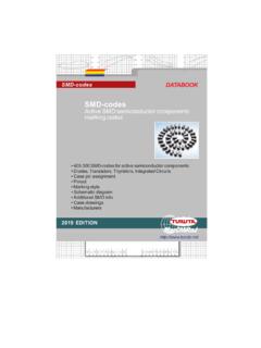
SMD-codes databook 2019 edition - Turuta
turuta.mdFor example, with a 6H SMD-code in a SOT-23 case might be either a npn-transistor BC818 (CDIL) or a capacitance-diode FMMV2104 (Zetex) or a n-channel jFET transistor MMBF5486 (Motorola) or a pnp-digital transistor MUN2131 (Motorola) or a pnp-digital transistor UN2117 (Panasonic) or a CMOS-integrated circuit- voltage detector with reset
Cleveland Institute of Electronics Electronics Symbols ...
www.cie-wc.edujfet, fet , emitter ase shielding common ground between two wires general (electric or magnetic optical shielding n— channel p- base shielded assembly ... dual diode with filament cathode gas-filled continued diode- bean power triode— hexode duo-diode- triode diode-triode— pentode eye high voltage rectifier next page

OPA657 1.6-GHz, Low-Noise, FET-Input Operational Amplifier ...
www.ti.com• ADC Input Amplifier The JFET input contributes virtually no current noise • Test and Measurement Front End while for broadband applications, a low voltage noise is also required. The low 4.8 nV/√Hz input voltage • High Gain Precision Amplifier noise provides exceptional input sensitivity for higher
Analog Electronics Laboratory Manual - 10ESL37
www.gopalancolleges.comJFET Characteristics and Amplifiers. MOSFET Characteristics and Amplifiers. Power Amplifiers. RC-Phase shift, Hartley, Colpitts and Crystal Oscillators Course outcomes: Through this course, the students: Acquire a basic knowledge in solid state electronics including diodes, MOSFET, BJT, and operational amplifier.

14. Transistor Characteristics Lab
www.hunter.cuny.eduthe terminals is a little different for the JFET.) Recall that a diode consists of a n doped (or excess ... Vcb +0.7 = Vce (5) The transistor characteristics are useful in amplifier design as well as understanding how transistors operate. The data below were collected for the example of a npn 2N36443 transistor using the circuit
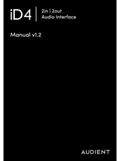
Manual v1
d9w4fhj63j193.cloudfront.netAudio Interface Inside the box: • iD4 • USB-C to USB-C cable • 16Printed Quick Start Guide Features include: • 1 x Audient Console Mic Pre • Class Leading Converters • 1 x JFET Instrument Input • 2 x Line Outputs • Dual Headphone Outputs • Firmware UpdateScrollcontrol • Speaker on/off Button • Monitor Mix and Pan
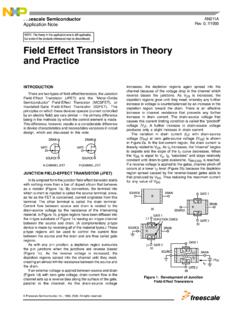
Field Effect Transistors in Theory and Practice ...
www.nxp.comreversed and the channel begins to deplete of carriers as seen in Figure 8. As with the JFET, drain-current flow depletes the channel area nearest the drain first. The structure of Figure 7, therefore, is both a depletion-mode and an enhancement-mode device. MODES OF OPERATION There are two basic modes of operation of FET’s — depletion and ...
Power MOSFET Basics: Understanding MOSFET Characteristics ...
www.vishay.combackside. The channel is formed under the polysilicon gate layer along the planar surface. However, the planar structure has an effective finite level of cell density because the JFET pinch-off effect 3 leads to an increased device on-resistance, compared with the Trench structure, at very high cell densities.
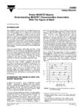
Precision, Very Low Noise, Low Input Bias Current, Wide ...
www.analog.comThe AD8510/AD8512/AD8513 are single-, dual-, and quad-precision JFET amplifiers that feature low offset voltage, input bias current, input voltage noise, and input current noise. The combination of low offsets, low noise, and very low input bias currents makes these amplifiers especially suitable for high
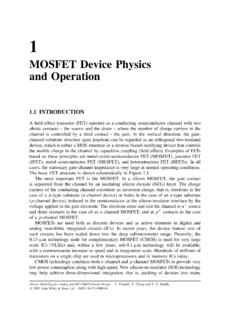
MOSFET Device Physics and Operation
homepages.rpi.eduthe mobile charge in the channel by capacitive coupling (field effect). Examples of FETs based on these principles are metal-oxide-semiconductor FET (MOSFET), junction FET (JFET), metal-semiconductor FET (MESFET), and heterostructure FET (HFETs). In all cases, the stationary gate-channel impedance is very large at normal operating conditions.
Welcome to the SMD Codebook - FaiDaTePc
www.faidatepc.itp13 PMBFJ113 Phi F SOT23 n-ch jfet J113 13A MMBD1503A Nat D SOT23 dual Si diode 200V 100mA 13A PZM13NB2A Phi A SOT346 dual ca 13V 0.3W zener 13E ZC2813E Zet A SOT23 dual ca RF schottky15V 20mA 13V PZM13NB Phi C SOT346 13V 0.3W zener 13Y BZV49-C13 Phi O SOT89 13V 1W zener 14s BAS125-04 Sie D SOT23 Dual series Schottky 25V 100mA
International Transistor Equivalents Guide
worldradiohistory.comC complementary transistor NPN/PNP DG dual germanium transistor DJ dual junction transistor DS dual silicon transistor FET field effect transistor G germanium transistor GD germanium Darlington transistor J junction FET (JFET) M MOSFET ME multiple -emitter transistor MOS metal oxide semiconductor P photo -transistor PU programmable unijunction ...
ディスクリート半導体の基礎
toshiba.semicon-storage.com(jfet) 抵抗内蔵型トランジスタ. 絶縁ゲートバイポーラトランジスタ. トランジスタ. トランジスタは、大別するとバイポーラ型、電界効果型および絶縁ゲートバイポーラ型の3種類に分 類される半導体デバイスです。
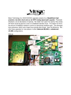
Music Technology Inc. SACD/CD/DAC upgrades consist of our ...
musictechnology.comprecision, low jitter clock and our all JFET analog signal path upgrade. Practically all players use an abundance of opamps. No matter how “good’ the opamp, they simply will never sound as good as a low or no feedback discrete circuit. The reason for this is the amount of feedback needed to control an operational amplifiers gain. This damages
El transistor de efecto de campo (FET) es un ejemplo de un ...
www.electronicasi.comJFET y de los MOSFET de tipo decremental permiten un análisis similar de cada uno en el dominio de dc. La diferencia mas importante entre los dos es el hecho de que el MOSFET de tipo decremental permite puntos de operación con valores positivos de V GS y niveles de I D que exceden I DSS. De hecho, para todas las configuraciones realizadas

AN-32 FET Circuit Applications
www.ti.comTL/H/6791–16 Level-Shifting-Isolation Amplifier The 2N4341 JFET is used as a level shifter between two op amps operated at different power supply voltages.
Similar queries
Junction field effect transistor JFET, Junction field-effect transistor JFET, Transistor, JFET input, JFET Input Operational, Operational, JFET, Input, Noise JFET quad operational amplifier, Low input, Field Effect Transistors, Channel, Operational amplifiers, JFET-input operational, JFET operational amplifiers, Amplifiers, FIELD, EFFECT, Enhancement mode, Noise, JFET Operational Amplifier, Analog Devices, Audio, Performance Audio, Performance, ADA4610, Junction Field Effect Transistor, Junction field-effect transistor, ADTL082, Precision, Precision JFET, 2N3819 JFET VHF/UHF Amplifier, ENHANCED-JFET LOW-OFFSET OPERATIONAL, ENHANCED-JFET LOW-OFFSET OPERATIONAL AMPLIFIERS, TEXAS, LF147/LF347 Wide Bandwidth Quad JFET Input Operational, LF147, LF347, Bandwidth Dual JFET Input Operational, Amplifier, Lecture 19: CMOS Operational Amplifiers, Junction transistor, Jfet junction field effect transistor, JFET transistor, Dual, Analog Electronics Laboratory Manual, Characteristics, Junction FET, Field effect transistor, AN-32 FET Circuit Applications