Transcription of 14. Transistor Characteristics Lab
1 14. Transistor Characteristics LabIntroduction Transistors are the active component in various devices like amplifiers and oscillators. They arecalled active devices since transistors are capable of amplifying (or making larger) signals. The proper-ties of transistors will be studied in this module so basically the focus here is understanding how transis-tors work. The next module will focus on basic amplifier design. Transistors can also be used as switchesbut since this is not a course in digital electronics, we will not discuss the function of transistors. Basic Bipolar Transistor Theory The basic Bipolar Transistor or BJT is two diodes constructed back to back on a piece of silicon.(Another kind of Transistor is the Junction Field Effect Transistor of jfet . The theory and labeling ofthe terminals is a little different for the jfet .) Recall that a diode consists of a n doped (or excessnegative current carriers) and a p doped (or excess positive current carriers) semiconductor.
2 The diodebiased in the forward or conducting direction appearswhile a diode in a circuit so that it is nonconducting or reverse direction TransistorThe basic Transistor consists of two diodes back to back. If the two p doped regions are next toeach other then and what results is a npn Transistor . Two laboratory diodes wired back-to-back will NOT make a transis-tor. In a real Transistor , the region of the two p regions is very narrow or thin so that the carriers candiffuse across the region freely. The symbol for the npn Transistor isBipolar transistors have three terminals: base, emitter, and collector. DEVICE FOR REMEMBERING: The arrow on the npn Transistor is Not Pointed iN. When the batteryis attached to the base-emitter junction of the npn Transistor as indicated below, current will flow as thebase-emitter junction is in the forward direction. can calculate the base current Ib using (1)Vbattery=IbR+Vbewhere Vbe= for silicon.
3 In the above diagram, the battery voltage is labeled example,suppose the battery voltage is Vbattery=12 Volts and R= kW then the base current is from equation (1)(2)Ib=Vbattery-VbeR= Mathematica you have the following different Transistor does NOT flow is the above circuit. The base-emitter junction is biased in the forward directionHOWEVER, the base-collector junction is in the REVERSE direction so no current the Base-Emitter Junction Combine the previous two circuits so that base-emitter junction is in the forward direction so for anpn Transistor we would place the battery thusThe surprising thing about transistors is that when a base current flows (because the base-emitter junctionis biased in the forward direction as above) then a collector current will also flow even though the base-collector junction is biased in the reverse direction. Also, the collector current is much larger than thebase current.
4 This is called Transistor ACTION and is the single most outstanding property above argument makes it intuitively clear that the emitter current is greater than the base current(also see equation #3 below). A property of transistors is that the surprising thing about transistors is that when a base current flows (because the base-emitter junctionis biased in the forward direction as above) then a collector current will also flow even though the base-collector junction is biased in the reverse direction. Also, the collector current is much larger than thebase current. This is called Transistor ACTION and is the single most outstanding property above argument makes it intuitively clear that the emitter current is greater than the base current(also see equation #3 below). A property of transistors is that the ratiob=IcIbis always a constant regardless of the size of Ic or Ib.
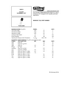
5 This ratio is typically in the range 100<b<300 andis the basis of the current amplification property of base current is said to CONTROL thecollector current since the size of Ib determines the size of Ic. It also follows from the above equationthat when Ib=0 then Ic= : Suppose b=100 and Ib= How large is Ic?b=100.;Ib= ;Ic=b* the collector current is much larger than the base TransistorWhen the two n regions are next to each other (as below) then one has a pnp should be clear that one of the diodes in a Transistor is in the forward direction emitter-collector whileone of the diodes is in the reverse direction. The symbol for the pnp Transistor the direction of the arrow is reverse from the npn Transistor . Transistors like the 2N2222 or PN2907 come in a variety of cases and either metal or plastic. One styleis of plastic case or package is indicated belowor just the bottom view isAnother style plastic case (view from below) appearsFinally the view from the bottom of a Transistor in a metal package A Simple Circuit for Measuring Transistor A Simple Circuit for Measuring Transistor Characteristics As we said, bipolar transistors have three terminals: base, emitter, and collector.
6 Transistorscharacteristics are graphs of the various currents (Ibis current into the base, Ie is current out of theemitter, and Icis current into collector) and voltages. Conservation of charge yields(3)Ib+Ic=Ie This means we need to measure only two currents as the other is determined from equation (1). Actuallythe base current is usually quite small compared with the other two currents and to a good approximationIc@Ie and this is worthwhile , involved are the voltages measured between the terminals:Vce=collector-emittervoltageVc b=collector-basevoltage Vbe=base-emittervoltage= These voltage should be measured with you digital VOM meter instead of using the oscilloscopesince at least for this lab we are interested in the DC voltages. (Also, if you use an oscilloscope you haveto be mindful of ground problems. More on this next lab. ) The base-emitter junction is biased in the forward direction so only the intrinsic voltage dropacross a pn junction appears.
7 This voltage drop is a constant for a silicon based junction. (If lesscommon germanium is used instead of silicon, the voltage drop is volts) Conservation of potential yields (4)Vcb+Vbe=VceThis means we need to measure only two voltages as the others are given by equation (2). Actually weneed measure only one voltage since Vbe= volts for silicon. (Remember the base-emitter junction is inthe forward direction.) Equation (2) can be written for a silicon Transistor (5)Vcb+ Transistor Characteristics are useful in amplifier design as well as understanding how transistorsoperate. The data below were collected for the example of a npn 2N36443 Transistor using the circuitbelow. (You will be using a 2N2222 Transistor so your data will be different.) battery was 9 volts and is the power supply in the lab. The fixed resistor is 1 kW while the variableresistor is actually several fixed resistors with the values indicted as RB in the table below.
8 The fixedresistor is called the collector resistor and has the value RC=1kW in the above circuit. If you use a pnp Transistor , reverse the polarity of the battery. The base-emitter voltage can becalculated using the battery voltage Vbattery and subtracting the voltage drop across the base resistor(assuming you have recorded the current Ib By the way, for the 2N2222 Transistor you will use, Ib is inthe mA range.).Characteristic Data:RBIb@ we graph the base current Ib versus collector current Ic ;Notice in the graph below that when the base current Ib is zero, the collector current Ic is also @BCdata,PlotStyle 8"Ib@mAD","Ic@mAD"<D20406080Ib@mAD2468Ic @mAD Graphics All the data fall on a straight line (regardless of the value of VCE) and the slope of the line is b given by(6)b=DIcDIborb=IcIbsince one data point can be taken as Ib=IC=0. Equation (6) is sometimes called "the Transistor Equa-tion" since it is so important to understanding how transistors work.
9 The numerical value of b for theabove Transistor *10-3H45-40L* : b is called hfe on the digital multimeter when you measure the Transistor characteristic. Thecollector-emitter voltage Vce and collector current Ic data isVcIcdata= ;and the graph of the graph of the collector voltage Vce versus the collector current Ic is a straight lineListPlot@VcIcdata,PlotStyle 8"Vce@VoltsD","Ic@mAD"<D2468 Vce@VoltsD2468Ic@mAD Graphics From equation (6) if we know the value of IC in the above graph, then IB=IC b. Since b=100 forexample, IB<<IC. Suppose for example IC=10 mA and b=100, then IB= the way, if you do a series of measurements of IC versus VCE all with the same IB and you plotthe results on the above graph, then you will get a horizontal straight line. The reason is that IB deter-mines IC regardless of the value of above graph is sometimes called the "load line" since the slope is determined by the value ofRC (see below) which often is the load resistor for the Transistor equation (6) if we know the value of IC in the above graph, then IB=IC b.
10 Since b=100 forexample, IB<<IC. Suppose for example IC=10 mA and b=100, then IB= the way, if you do a series of measurements of IC versus VCE all with the same IB and you plotthe results on the above graph, then you will get a horizontal straight line. The reason is that IB deter-mines IC regardless of the value of above graph is sometimes called the "load line" since the slope is determined by the value ofRC (see below) which often is the load resistor for the Transistor the Collector Voltage Vce: The collector voltage Vce is determined in the above experiment directly with a meter. However,this voltage can also be easily calculated as we shall see. First calculate the base current Ib using (7)Vbattery=IbRB+Vbeand thus(8)Ib=Vbattery-VbeRBVbe= for silicon transistors and the battery voltage is usually fixed IVbattery=9V in the aboveexample) so Ib is determined by RB.