Transcription of Dual N-Channel JFET Switch
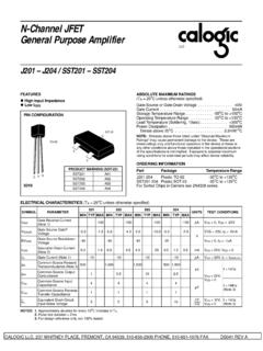
1 Dual N-Channel jfet SwitchU401 U406 FEATURES Minimum System Error and Calibration Low Drift With Temperature Operates From Low Power Supply Voltages High Output ImpedanceABSOLUTE MAXIMUM RATINGS(TA = 25oC unless otherwise specified)Gate-Drain or Gate-Source Voltage .. 50 VGate Current (Note 1) .. 10mAStorage Temperature Range .. -65oC to +200oCOperating Temperature Range .. -55oC to +150oCLead Temperature (Soldering, 10sec) .. +300oCOne SideBoth SidesPower Dissipation (TA = 85oC)300mW500mW Derate above : Stresses above those listed under "Absolute MaximumRatings" may cause permanent damage to the device. These arestress ratings only and functional operation of the device at these orany other conditions above those indicated in the operational sectionsof the specifications is not implied. Exposure to absolute maximumrating conditions for extended periods may affect device INFORMATIONPartPackageTemperature RangeU401-6 Hermetic TO-71-55oC to +150oCXU401-6 Sorted Chips in Carriers-55oC to +150oCLLCPIN CONFIGURATIONS2G1D2D1G2S1TO-71CJ2 ELECTRICAL CHARACTERISTICS (TA = 25oC unless otherwise specified)SYMBOLPARAMETERU401U402U403U40 4U405U406 UNITSTEST CONDITIONSMINMAXMINMAXMINMAXMINMAXMINMAX MINMAXBVGSSGate-SourceBreakdown Voltage-50-50-50-50-50-50 VVDS = 0, IG = -1 AIGSSGate Reverse Current(Note 2)-25-25-25-25-25-25pAVDS = 0, VGS = -30 VVGS(off)Gate-Source = 15V, ID = 1nAVGS(on)Gate-Source Voltage(on) = 15V, ID = 200 AIDSSS aturation DrainCurrent (Note 3) = 10V, VGS = 0 IGOperating GateCurrent (Note 2)
2 -15-15-15-15-15-15pAVDG = 15V, ID = 200 A-10-10-10-10-10-10nATA = 125oCBVG1-G2 Gate-GateBreakdown Voltage 50 50 50 50 50 50 VVDS = 0, VGS = 0,IG = 1 AgfsCommon-SourceForwardTransconductance (Note 3)2000 7000 2000 7000 2000 7000 2000 7000 2000 7000 2000 7000 SVDS = 10V,VGS = 0f = 1kHzgosCommon-SourceOutput Conductance202020202020gfsCommon-SourceF orwardTransconductance1000 2000 1000 2000 1000 2000 1000 2000 1000 2000 1000 2000 VDG = 15V,ID = 200 Af = 1kHzgosCommon-SourceOutput Capacitance(Note 6) = 1 MHzCrssCommon-SourceReverse TransferCapacitance (Note 6) InputNoise Voltage202020202020nV HzVDS = 15V,VGS = 0f = 10Hz(Note 6)CMRRC ommon-ModeRejection Ratio9595959590dBVDG = 10 to 20V, ID = 200 A (Note 5, 6)| VGS1 VGS2 |DifferentialGate-Source Voltage5 1010152040mVVDG = 10V, ID = 200 A| VGS1 VGS2 | TGate-Source VoltageDifferential Drift (Note4)101025254080 V/oCVDG = 10V,ID = 200 ATA = -55oCTB = +25oCTC = +125oCNOTES: doubles for every 10oC increase in Pulse test duration = 300 s; duty cycle 3%.
3 At end points TA, TB, = 20 log10 VDD | VGS1 VGS2 | , VDD = design reference only, not 100% U406 LLC


