Search results with tag "Analog devices"

AD9826 Complete 16-Bit Imaging Signal ... - Analog Devices
www.analog.com22 VINB AI Analog Input, Blue Channel 23 CML AO Internal Bias Level Decoupling 24 VING AI Analog Input, Green Channel 25 OFFSET AO Clamp Bias Level Decoupling 26 VINR AI Analog Input, Red Channel TYPE: AI = Analog Input, AO = Analog Output, DI = Digital Input, DO = Digital Output, P = Power. PIN CONFIGURATION TOP VIEW (Not to Scale) 28 27 26 25 ...

Low Cost, Low Power, Differential ADC ... - Analog Devices
www.analog.comlicense is granted by implication or otherwise under any patent or patent rights of Analog Devices. Trademarks and register ed trademarks are the property of their respective owners. One Technology Way, P.O. Box 9106, Norwood, MA 020629106, U.S.A. - Tel: 781.329.4700 www.analog.com Fax: 781.461.3113 ©2004–2012 Analog Devices, Inc.

HMC451LP3 / 451LP3E - Analog Devices
www.analog.comfor price, delivery, and to place orders: Analog Devices, inc., one Technology way, p.o. Box 9106, norwood, mA 02062-9106 phone: 781-329-4700 • order online at www.analog.com Application support: phone: 1-800-AnAloG-D Amplifiers - l ine A r & p ower - sm T 2 HMC451LP3 / 451LP3E v02.0121 GaAs PHEMT MMIC MEDIUM POWER AMPLIFIER, 5 - 18 GHz
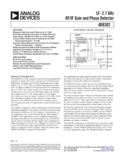
AD8302 LF 2.7 GHz RF/IF Gain and Phase ... - Analog Devices
www.analog.comInformation furnished by Analog Devices is believed to be accurate and reliable. However, no responsibility is assumed by Analog Devices for its ... The AD8302 is a fully integrated system for measuring gain/loss and phase in numerous receive, transmit, and instrumentation ... Slope From Linear Regression 29 mV/dB Deviation vs. Temperature ...

DC/DC CONTROLLER - Analog Devices
www.analog.com4 DC/DC Controller LTspice LTspice® is a high performance SPICE simulation software, schematic capture and waveform viewer with enhancements and models for easing the simula- tion of analog circuits. Included in the download of LTspice are macromodels for a majority of Analog Devices’ switching regulators, amplifiers, as well as a

2 A, Ultralow Noise, High PSRR, RF Linear Regulator Data ...
www.analog.comHigh PSRR, RF Linear Regulator Data Sheet ADP7158 Rev. C Document Feedback Information furnished by Analog Devices is believed to be accurate and reliable. However, no responsibility is assumed by Analog Devices for its use, nor for any infringements of patents or other rights of third parties that may result from its use.
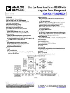
Ultra Low Power Arm Cortex-M3 MCU with Integrated Power ...
www.analog.comIntegrated Power Management Data Sheet ADuCM3027/ADuCM3029 Rev. B Document Feedback Information furnished by Analog Devices is believed to be accurate and reliable. However, no responsibility is assumed by Analog Devices for its use, nor for any infringements of patents or other rights of third parties that may result from its use.

25 MHz to 3000 MHz Fractional-N PLL with Integrated VCO ...
www.analog.comFractional-N PLL with Integrated VCO Data Sheet HMC832A Rev. B Document Feedback Information furnished by Analog Devices is believed to be accurate and reliable. However, no responsibility is assumed by Analog Devices for its use, nor for any infringements of patents or other rights of third parties that may result f rom its use.

15 MHz Rail-to-Rail Operational Amplifiers Data Sheet ...
www.analog.com15 MHz Rail-to-Rail Operational Amplifiers Data Sheet OP162/OP262/OP462 Rev. H Document Feedback Information furnished by Analog Devices is believed to be accurate and reliable. However, no responsibility is assumed by Analog Devices for its use, nor for any infringements of patents or other rights of third parties that may result from its use.

4-Channel, Low Noise, Low Power, 24-Bit, Sigma-Delta ADC ...
www.analog.comSigma-Delta ADC with PGA and Reference Data Sheet AD7124-4 Rev. D Document Feedback Information furnished by Analog Devices is believed to be accurate and reliable. However, no responsibility is assumed by Analog Devices for its use, nor for any infringements of patents or other rights of third parties that may result from its use.

LC2MOS 16-Bit Voltage Output DAC Data Sheet AD7846
www.analog.comData Sheet AD7846 Rev. H Document Feedback Information furnished by Analog Devices is believed to be accurate and reliable. However, no responsibility is assumed by Analog Devices for its use, nor for any infringements of patents or other rights of third parties that may result from its use. Specifications subject to change without notice. No

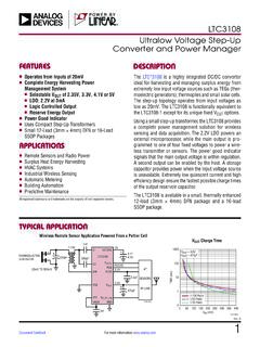
LT8364 (Rev. A) - Analog Devices
www.analog.comLT8364 1 ev A Document Feedback For more information www.analog.com DESCRIPTION TYPICAL APPLICATION FEATURES Low IQ Boost/SEPIC/ Inverting Converter with 4A, 60V Switch The LT®8364 is a current mode DC/DC converter with a 60V, 4A switch operating from a 2.8V to 60V input.

1 MHz to 2.7 GHz RF Gain Block Data Sheet AD8354
www.analog.com1 MHz to 2.7 GHz RF Gain Block Data Sheet AD8354 Rev. F Document Feedback Information furnished by Analog Devices is believed to be accurate and reliable. However, no responsibility is assumed by An alog Devices for its use, nor for any infringements of patents or other rights of third parties that may result from its use.

MT-014: Basic DAC Architectures I: String ... - Analog Devices
www.analog.comMT-014 TUTORIAL. Basic DAC Architectures I: String DACs and . Thermometer (Fully Decoded) DACs . by Walt Kester. INTRODUCTION . Rather than simply treating DACs as black boxes having a digital input and an analog output, it

LT1716 (Rev. B) - Analog Devices
www.analog.comLT1716 3 Rev For more information www.analog.com ELECTRICAL CHARACTERISTICS The l denotes the specifications which apply over the full operating temperature range of –40°C ≤ TA ≤ 85°C, otherwise specifications are at TA = 25°C. Single supply operation V+ = 5V, V– = 0V; VCM = V+/2 unless otherwise noted.(Note 4)
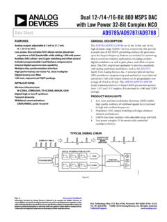
Dual 12-/14-/16-Bit 800 MSPS DAC with Low Power 32-Bit ...
www.analog.comwith analog quadrature modulators, such as the ADL5375 family from Analog Devices, Inc. A serial peripheral interface (SPI) provides for programming and readback of many internal parameters. Full-scale output current can be programmed over a range of 10 mA to 30 mA. The AD9785/AD9787/AD9788

LT3970 Series (Rev. D) - Analog Devices
www.analog.com5 Rev. D For more information www.analog.com LT3970 Series TYPICAL PERFORMANCE CHARACTERISTICS Efficiency, VOUT = 3.3V Efficiency, VOUT = 5V LT3970 Feedback Voltage TA = 25°C, unless otherwise noted. D RR 50 70 90 40 60 80. 1 10 100 30 20. VIN R TION
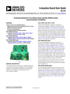
Evaluation Board User Guide - Analog Devices
www.analog.comEvaluation Board User Guide UG-364 One Technology Way • P.O. Box 9106 • Norwood, MA 02062-9106, U.S.A. • Tel: 781.329.4700 • Fax: 781.461.3113 • www.analog.com Evaluating the AD5933 1 MSPS, 12-Bit Impedance Converter Network Analyzer PLEASE SEE THE LAST PAGE FOR AN IMPORTANT WARNING AND LEGAL TERMS AND CONDITIONS. Rev. 0 | Page 1 …
LTC6908-1/LTC6908-2 (Rev. C) - Analog Devices
www.analog.comLTC6908-1/LTC6908-2 3 Re C For more information www.analog.com The l denotes the specifications which apply over the full operating temperature range, otherwise specifications are at TA = 25°C. Test conditions are V+ = 2.7V to 5.5V, RL = 5k, CL = 5pF unless otherwise noted.

3 MSPS, 12-/10-/8-Bit ADCs in 6-Lead TSOT ... - Analog Devices
www.analog.comlow power, successive approximation analog-to-digital converters (ADCs), respectively. The parts operate from a single 2.35 V to 3.6 V power supply and feature throughput rates of up to 3 MSPS. The parts contain a low noise, wide bandwidth track-and-hold amplifier that can handle input frequencies in excess of 55 MHz.

锁相环常见问题解答 - Analog Devices
www.analog.com锁相环常见问题解答 亚洲技术支持中心 电话:4006 100 006 Email:china.support@analog.com 5 第1章 简介 1.1 ADI 公司锁相环产品概述 ADI 是高性能模拟器件供应商,在锁相环领域已有十多年的的设计经验。

AN-686 APPLICATION NOTE - Analog Devices
www.analog.comI2C state machine will determine the effectiveness of the clocking approach.) The method is quite simple. It is the master’s job to recover the bus and restore control to the main program. When the master detects the SDA line stuck in the low state, it merely needs to send some additional clocks and gener-ate a STOP condition.
LT3120 (Rev. 0) - Analog Devices
www.analog.comMonolithic Buck-Boost Converter The LT®3120 is a high efficiency 26V monolithic buck-boost converter. Extensive feature integration and very low resistance internal power switches minimize the total solution footprint for even the most demanding applica-tions. A proprietary 4-switch PWM architecture provides

Transimpedance Amplifiers for Wide Range ... - Analog Devices
www.analog.comThe LTC6268 offers 500MHz gain bandwidth, enabling the single-stage circuits shown in the LTC6268 data sheet from 20kΩ transimpedance gain with 65MHz bandwidth to 499kΩ transimpedance gain with 11.2MHz bandwidth. With just 0.45pF input capacitance, the LTC6268 contributes only a small portion of the total circuit capacitance, preserving high
ADIN1300 (Rev. 0) - Analog Devices
www.analog.comCrystal oscillator frequency/25 MHz clock input frequency (50 MHz for RMII) 25 MHz/125 MHz synchronous clock output . Small package and wide temperature range . 40-lead, 6 mm × 6 mm LFCSP . Specified for −40°C to +105°C ambient operation . Low power consumption . 330 mW for 1000BASE-T . 140 mW for 100BASE-TX

Single-/Dual-Supply, High Voltage Isolated IGBT Gate ...
www.analog.comIGBT Gate Driver with Miller Clamp Data Sheet ADuM4135 Rev. D Document Feedback Information furnished by Analog Devices is believed to be accurate and reliable. However, no ... 5 kV ac for 1 minute per UL 1577 . CSA Component Acceptance Notice 5A . DIN V VDE V 0884-10 (VDE V 0884-10):2006-12 . V IORM = 849 V peak (reinforced/basic)
LT4356-3 (Rev. D) - Analog Devices
www.analog.comBack-to-back FETs can be used in lieu of a Schottky diode for reverse input protection, reducing voltage drop and power loss. The SHDN input turns off the part, including the auxiliary amplifier, and reduces the quiescent current to less than 7µA. n Automotive/Avionic Surge Protection n Hot Swap/Live Insertion
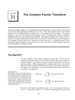
The Real DFT - Analog Devices
www.analog.comIn Chapter 8 we defined the real version of the Discrete Fourier Transform according to the equations: In words, an N sample time domain signal, x [n], is decomposed into a set of N /2 %1 cosine waves, and N /2 %1 sine waves, with frequencies given by the.
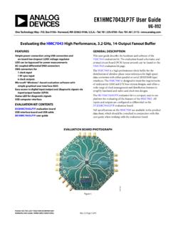
EK1HMC7043LP7F User Guide - Analog Devices
www.analog.com1. Apply 0 V to VCCIN (TP14). 2. Apply 3.3 V to 3.3V_MAIN (TP15). 3. Remove R245 and FB20. 4. Populate R12 (to isolate the serial peripheral interface (SPI) board current consumption from the HMC7043). Connect a bench 3.3 V power supply to each of the supply pins on the 3.3 V main headers (TP15 and TP16).
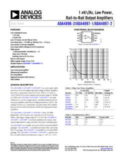
1 nV/√Hz, Low Power, Rail-to-Rail Output Amplifiers Data ...
www.analog.comAnalog Devices, Inc., proprietary next-generation SiGe bipolar process and innovative architecture enable such high performance amplifiers. The ADA4896-2/ADA4897-1/ADA4897-2 have 230 MHz bandwidth, 120 V/μs slew rate, and settle to 0.1% in 45 ns. With a wide supply voltage range of 3 V to 10 V, the ADA4896-2/

LT1615/LT1615-1 DC/DC Converters - Analog Devices
www.analog.comoff-time is increased to 1.5µs and the current limit is reduced to around 250mA (70% of its normal value). This reduces the average inductor current and helps minimize the power dissipation in the LT1615 power switch and in the external inductor and diode. The LT1615-1 operates in the same manner, except the switch current is limited to

RGB to NTSC/PAL Encoder AD724 - Analog Devices
www.analog.comAD724–SPECIFICATIONS –2– REV. B (Unless otherwise noted, V S = +5, T A = +258C, using FSC synchronous clock.All loads are 150 V 6 5% at the IC pins. Outputs are measured at the 75 V reverse terminated load.) Parameter Conditions Min Typ Max Units

FEATURES DESCRIPTIO U - Analog Devices
www.analog.comCMRR Common Mode Rejection Ratio VCM = 0.1V to 3.2V 90 103 87 102 dB PSRR Power Supply Rejection Ratio VS = ±2V to ±18V, VO = 0V 100 117 97 116 dB Maximum Output Voltage Swing Output Low, 600Ω to GND 615 6 18 mV Output High, 600Ω to GND 3.2 3.8 3.1 3.8 V IS Supply Current 380 630 400 680 µA
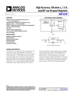
High Accuracy, Ultralow I , 1.5 A, anyCAP ... - Analog Devices
www.analog.coma load current up to 1.5 A. The ADP3339 stands out from the conventional LDOs with a novel architecture and an enhanced process that enables it to offer performance advantages and higher output current than its competition. Its patented design requires only a 1.0 μF output capacitor for stability. This device

215MHz, Rail-to-Rail Output, 1.1nV/ - Analog Devices
www.analog.com1 623012fc LT6230/LT6230-10 LT6231/LT6232 Typical applicaTion FeaTures DescripTion 215MHz, Rail-to-Rail Output, 1.1nV/√Hz, 3.5mA Op Amp Family The LT®6230/LT6231/LT6232 are single/dual/quad low noise, rail-to-rail output unity-gain stable op amps that

Two Selectable Inputs, 12 LVPECL Outputs, SiGe Clock ...
www.analog.comthe Analog Devices, Inc., proprietary XFCB3 silicon germa-nium (SiGe) bipolar process. This device is designed for high speed applications requiring low jitter. The device has two selectable differential inputs via the IN_SEL control pin. Both inputs are equipped with center tapped, differential, 100 Ω on-chip termination resistors. The inputs
CN-0385 - Analog Devices
www.analog.com(ADC) 驱动器,以及一个用于采样有效通道信号的18 位、 2.0 MSPS精密PulSAR® ADC。提供0.4、0.8、1.6 和3.2 增 益配置。 turbo模式下,系统最大采样速率为2 MSPS;正常模式下为 1.5 MSPS。通道切换逻辑与ADC 转换同步,最大通道切换 速率为1.5 MHz。
HMC542BLP4E - Analog Devices
www.analog.comClock to Latch Enable tlsup 40 - ns Latch Enable Window, Latch Enable to C0.5 through C8 tpd - 30 ns Setup time from Reset to Shift Clock - 20 - ns Clock Frequency (1/tclk) fclk - 30 MHz Timing Serial Input Truth Table Latch Enable Shift Clock Reset Function X X l Shift register cleared X á H Shift register clocked á X H Contents of shift ...

HmC3653lp3Be - Analog Devices
www.analog.comsingle positive upply: +5V ... use rf circuit design techniques. ignal lines s should have 50 o hm impedance while the package ground leads and exposed paddle should be con-nected directly to the ground plane similar to that shown. A sufficient number of via holes should be
Evaluating the HMC7044 Dual Loop Clock Jitter Cleaner
www.analog.comevaluation software is C:\Program Files (x86)\Analog Devices\Jitter Attenuator\. 3. After the installation completes, the user is prompted to install the drivers for the USB interface. STARTING THE SOFTWARE After the evaluation software is installed, run the software as follows: 1. Power up and connect the evaluation board to the PC. 2.

5 V, Slew Rate Limited, Half-Duplex and Full Duplex RS-485 ...
www.analog.com5 V, Slew Rate Limited, Half-Duplex and Full Duplex RS-485/RS-422 Transceivers Data Sheet ADM4850 to ADM4857 Rev. F Document Feedback Information furnished by Analog Devices is believed to be accurate and reliable.
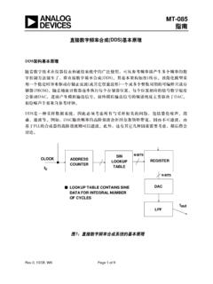
直接数字频率合成(DDS)基本原理 - Analog Devices
www.analog.com4,096 65,536 1,048,576 16,777,216 268,435,456 4,294,967,296 281,474,976,710,656 M = JUMP SIZE 图3:数字相位轮 Page 3 of 9 考虑n = 32,M = 1的情况。相位累加器会逐步执行2 32个可能的输出中的每一个,直至溢出 并重新开始。相应的输出正弦波频率等于输入时钟频率2 32分频。 …

ADXL103/ADXL203 (Rev. F) - Analog Devices
www.analog.comHigh performance, single-/dual-axis accelerometer on a single IC chip 5 mm × 5 mm × 2 mm LCC package 1 mg resolution at 60 Hz Low power: 700 μA at V S = 5 V (typical) High zero g bias stability High sensitivity accuracy −40°C to +125°C temperature range X and Y axes aligned to within 0.1° (typical) Bandwidth adjustment with a single ...
Evaluation Board User Guide - Analog Devices
www.analog.comUG-261 Evaluation Board User Guide Rev. C | Page 4 of 8 QUICK START FOR THE EVAL-INAMP-62RZ BOARD CIRCUIT OPTIONS Single-Supply Operation A jumper is provided to select between single or dual power supplies. The evaluation board is shipped with W14 in the dual-supply position. To convert to single supply, place W14 in the
LTC3108 (Rev. D) - Analog Devices
www.analog.comVOUT Quiescent Current VOUT = 3.3V, VOUT2_EN = 0V 0.2 µA VAUX Quiescent Current No Load, All Outputs Charged 6 9 µA LDO Output Voltage 0.5mA Load l 2.134 2.2 2.266 V LDO Load Regulation For 0mA to 2mA Load 0.5 1 % LDO Line Regulation For VAUX from 2.5V to 5V 0.05 0.2 % LDO Dropout Voltage ILDO = 2mA 100 200 mV LDO Current Limit VLDO = 0V l 4 ...

LTC6226/LTC6227 (Rev. 0) - Analog Devices
www.analog.comLow Distortion Rail-to-Rail Output Op Amps The LTC®6226/LTC6227 are very fast, low noise rail-to-rail output, unity gain stable single/dual op amps, with a gain-bandwidth product of 420MHz and a slew rate of 180V/μs. The low input referred voltage noise of only 1nV/√Hz and low distortion of less than 90d–BC for 4VP-P signals at
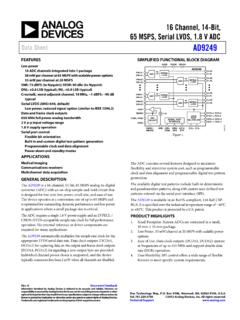
16 Channel, 14-Bit, 65 MSPS, Serial LVDS, 1.8 V ADC
www.analog.com16 Channel, 14-Bit, 65 MSPS, Serial LVDS, 1.8 V ADC Data Sheet AD9249 Rev. 0 Document Feedback Information furnished by Analog Devices is believed to be accurate and reliable.
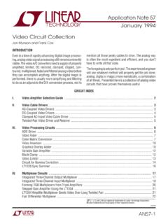
AN57 - Video Circuit Collection - Analog Devices
www.analog.comneed to have an appropriate offset applied to preserve linear amplifi er operation over the intended signal swing. For systems that lack an available negative supply, the LT1983-3 circuit shown in Figure 5 can be used to easily produce a local-use –3V that can simplify an overall cable-driving solu-

MT-046: Op Amp Settling Time - Analog Devices
www.analog.comsource capable of generating a pulse of sufficient flatness. In other words, if the op amp under test has a settling time of 20 ns to 0.1%, the applied pulse should settle to better than 0.05% in less than 5 ns. PULSE GENERATOR (50ΩOUTPUT) DUT 100Ω 100Ω 100Ω R2 R1 + – +0.5V –1.8V –1V 0V 50ΩCOAX "FLAT" REGION MAKE AS SHORT AS POSSIBLE ...
Similar queries
Analog Devices, Analog, Channel, Digital, HMC451LP3 / 451LP3E, Measuring, Linear, DC/DC Controller, Linear Regulator Data, Linear Regulator Data Sheet, Integrated, Management, Rights, Fractional-N PLL with Integrated VCO, Rail, OP162, Sigma, Delta ADC, Data, Data Sheet AD7846, LT8364, GHz RF Gain Block Data Sheet AD8354, An alog Devices, Architectures, LT1716, ADL5375, Performance, Efficiency, User Guide, To-digital converters, Master, LT3120, Buck, Power, Switch, Circuits, ADIN1300 Rev. 0, Clock, Clamp, FETs, The Real DFT, VCCIN, Generation, ADA4897, Current, Average, Rejection Ratio, PSRR Power Supply Rejection Ratio, Supply, Output current, Output, ApplicaTion, Silicon, PulSAR, Latch, Upply, Evaluating the HMC7044 Dual Loop Clock Jitter, Software, 4,096, Quiescent Current, LDO Current, Low noise, Voltage noise, 65 MSPS, Serial LVDS