Transcription of Evaluating the HMC7044 Dual Loop Clock Jitter Cleaner
1 EK1 HMC7044LP10B User GuideUG-826 One Technology Way P. O . Box 9106 Norwood, MA 02062-9106, Te l : Fax: Evaluating the HMC7044 dual Loop Clock Jitter Cleaner PLEASE SEE THE LAST PAGE FOR AN IMPORTANT WARNING AND LEGAL TERMS AND CONDITIONS. Rev. 0 | Page 1 of 10 FEATURES Simple power connection using USB connection and on-board LDO voltage regulators LDOs can be bypassed for power measurements AC-coupled differential SMA connectors SMA connectors for 2 reference Inputs 6 Clock outputs 1 VCXO output Microsoft Windows based evaluation software with simple graphical user interface On-board PLL loop filter Easy access to digital input/output and diagnostic signals via input/output header (4 GPIOs)
2 Status LEDs for diagnostic signals USB computer interface EVALUATION KIT CONTENTS EV3 HMC7044LP10B evaluation board USB interface board and USB cable EK1 HMC7044LP10B user guide GENERAL DESCRIPTION This user guide describe the hardware and software of the HMC7044 evaluation kit. The evaluation board schematic and printed circuit board (PCB) layout artwork can be found on the EK1 HMC7044LP10B product page at The HMC7044 meets the requirements of multicarrier GSM and LTE base station designs and offers a wide range of Clock management and distribution features to simplify baseband and radio card Clock tree designs.
3 The high performance dual -loop core of the HMC7044 enables the base station designer to attenuate the incoming Jitter of a primary system reference Clock , such as a CPRI source, with the help of the narrow-band configured first PLL loop, which disciplines an external VCXO, and to generate the low phase noise, high frequency clocks with the wider-band second PLL to drive data converter sample Clock inputs. The EV3 HMC7044LP10B evaluation board is a compact, easy to use platform for Evaluating all the features of the HMC7044 . A MHz VCXO is mounted on the evaluation board to provide a complete solution.
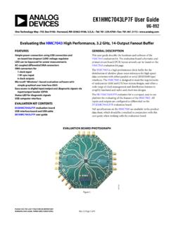
4 All inputs and outputs are configured as differential on the evaluation board. Full specifications on the HMC7044 are available in the product data sheet, which should be consulted in conjunction with this user guide when working with the evaluation board. EVALUATION BOARD PHOTOGRAPH 13041-001 Figure 1. UG-826 EK1 HMC7044LP10B User Guide Rev. 0 | Page 2 of 10 TABLE OF CONTENTS Features .. 1 Evaluation Kit Contents .. 1 General Description .. 1 Evaluation Board Photograph .. 1 Revision History .. 2 Evaluation Board Hardware .. 3 Checking Jumper Connections.
5 3 Setting Up the Power and PC Connections .. 3 Setting Up the Signal Connections .. 3 Bypassing the 5 V LDO Power Supply .. 3 Evaluation Board software Setup ..4 Installing the software ..4 Starting the software ..4 Evaluation Board software Operation ..5 Menu Bar of Main Window ..5 Using the software to Control the Functional Blocks of the HMC7044 ..6 PLL 2 Controls ..7 Output Channel Controls ..8 Quick Start Guide to the HMC7044 .. 10 REVISION HISTORY 9/15 Revision 0: Initial Version EK1 HMC7044LP10B User Guide UG-826 Rev. 0 | Page 3 of 10 EVALUATION BOARD HARDWARE The following instructions are for setting up the physical connections to the EV3 HMC7044LP10B evaluation board.
6 CHECKING JUMPER CONNECTIONS Remove all jumpers (JP2 and JP3). SETTING UP THE POWER AND PC CONNECTIONS Set up the power and PC connections as follows: 1. Install the HMC7044 evaluation software before connecting the evaluation board to the PC for the first time (see the Installing the software section). Administrative privileges are required for the installation. 2. Connect a 5 V supply voltage to Test Point TP38 of the evaluation board. 3. Connect the USB interface board to the evaluation board, as shown in Figure 2. 4. Connect the USB cable to the USB interface and the PC.
7 5. The Found New Hardware Wizard automatically appears when the USB interface is connected. Select Install the software automatically and then click Next. 6. The Found New Hardware Wizard may appear twice during the installation. See the Evaluation Board software section for details on running the HMC7044 board software . SETTING UP THE SIGNAL CONNECTIONS After setting up the power and PC connections, use the following procedure to set up signal connections: 1. Connect a signal generator to the CLKIN0_RFSYNC_P SMA Connector J11. By default, the reference inputs on the evaluation board are ac-coupled.
8 Terminate the CLKIN0_RFSYNC_N SMA Connector J10 with a 50 termination. An amplitude setting of 6 dBm from the signal generator is sufficient. 2. Connect an oscilloscope, spectrum analyzer, or other lab equipment to any output of the CLKOUTx_P or CLKOUTx_N SMA connectors. Place a 50 termination on all unused differential output pairs. BYPASSING THE 5 V LDO POWER SUPPLY The evaluation board contains three on-board, low dropout regulators (LDOs) to regulate 5 V to V supply domain. The evaluation board can be configured to bypass linear regulators, which is useful for measuring HMC7044 power consumption.
9 See the evaluation board schematics provided on the EK1 HMC7044LP10B product page at Bypass the 5 V two on-board LDOs for the HMC7044 as follows: 1. Remove the on-board LDOs (U2 and U4). 2. Populate R241, FB10, C105, C154, and C159 for VCC1_VCO. 3. Remove R245 and FB20. 4. Populate R12 (to isolate the SPI interface board current consumption from the HMC7044 ). Connect a bench V power supply to each of the supply pins on the V main header (TP15). Note that it is very important to not have the 5 V supply connected to TP15 of the evaluation board.
10 Connect a bench V power supply to TP38 for the on-board LDO of the VCXO supply, VCC_VCXO. 13041-002 Figure 2. HMC7044 Evaluation Kit Setup UG-826 EK1 HMC7044LP10B User Guide Rev. 0 | Page 4 of 10 EVALUATION BOARD software SETUP Follow the instructions included in this section to set up the HMC7044 evaluation software . INSTALLING THE software Do not connect the evaluation board until the software installation is completed. 1. Download the installer from HMC7044 product page at 2. Double-click from the installer file. Follow the installation instructions.
