Transcription of LT1173 - Micropower DC/DC Converter Adjustable …
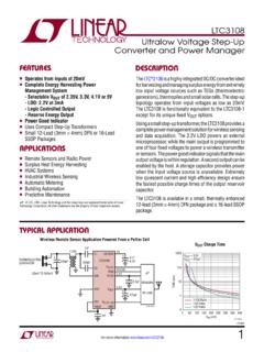
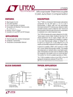
1 LT1173 . Micropower DC/DC Converter Adjustable and Fixed 5V, 12V. U. FEATURES DESCRIPTIO. Operates at Supply Voltages From to 30V The LT1173 is a versatile Micropower DC-DC Converter . Consumes Only 110 A Supply Current The device requires only three external components to Works in Step-Up or Step-Down Mode deliver a fixed output of 5V or 12V. Supply voltage ranges Only Three External Components Required from to 12V in step-up mode and to 30V in step-down Low Battery Detector Comparator On-Chip mode. The LT1173 functions equally well in step-up, step- User- Adjustable Current Limit down or inverting applications.
2 Internal 1A Power Switch Fixed or Adjustable Output Voltage Versions The LT1173 consumes just 110 A supply current at Space Saving 8-Pin MiniDIP or SO8 Package standby, making it ideal for applications where low quies- cent current is important. The device can deliver 5V at UO 80mA from a 3V input in step-up mode or 5V at 200mA. APPLICATI S from a 12V input in step-down mode. Flash Memory Vpp Generators Switch current limit can be programmed with a single 3V to 5V, 5V to 12V Converters resistor. An auxiliary gain block can be configured as a low 9V to 5V, 12V to 5V Converters battery detector, linear post regulator, under voltage lock- LCD Bias Generators out circuit or error amplifier.
3 Peripherals and Add-On Cards Battery Backup Supplies For input sources of less than 2V, use the LT1073. Laptop and Palmtop Computers Cellular Telephones Portable Instruments and LTC are registered trademarks and LT is a trademark of Linear Technology Corporation. UO. TYPICAL APPLICATI S. Logic Controlled Flash Memory VPP Generator VPP Output L1*. 100 H 1N5818. 5 VIN 12V. 100mA. 47 . VOUT. 5V/DIV. I LIM V IN. SW1 . 0V. + + SANYO. 10 F LT1173 OS-CON. 100 F. FB. PROGRAM. GND SW2 5V/DIV. 124k . 5ms/DIV. 1173 TA02. 1N4148. PROGRAM. LT1173 TA01. *L1 = GOWANDA GA20-103K EFFICIENCY = 81%. COILTRONICS CTX100-4 = 1% METAL FILM.
4 NO OVERSHOOT. 1. LT1173 . W W W U U W U. ABSOLUTE AXI U RATI GS PACKAGE/ORDER I FOR ATIO. Supply Voltage (VIN) .. 36V TOP VIEW. SW1 Pin Voltage (VSW1) .. 50V ORDER PART. ILIM 1 8 FB (SENSE)* NUMBER. SW2 Pin Voltage (VSW2) .. to VIN VIN 2 7 SET. Feedback Pin Voltage ( LT1173 ) .. 5V SW1 3 6 AO LT1173CN8. Sense Pin Voltage ( LT1173 , -5, -12) .. 36V SW2 4 5 GND LT1173CN8-5. Maximum Power Dissipation .. 500mW LT1173CN8-12. N8 PACKAGE. Maximum Switch Current .. 8-LEAD PLASTIC DIP. Operating Temperature Range .. 0 C to 70 C *FIXED VERSIONS. TJMAX = 90 C, JA = 130 C/W. Storage Temperature Range .. 65 C to 150 C.
5 TOP VIEW. Lead Temperature, (Soldering, 10 sec.).. 300 C LT1173CS8. ILIM 1 8 FB (SENSE)*. LT1173CS8-5. Consult factory for Industrial and Military grade parts VIN 2 7 SET. LT1173CS8-12. SW1 3 6 AO. SW2 4 5 GND S8 PART MARKING. S8 PACKAGE 1173. 8-LEAD PLASTIC SOIC. *FIXED VERSIONS. 11735. TJMAX = 90 C, JA = 150 C/W 117312. ELECTRICAL CHARACTERISTICS TA = 25 C, VIN = 3V, unless otherwise noted. SYMBOL PARAMETER CONDITIONS MIN TYP MAX UNITS. IQ Quiescent Current Switch Off 110 150 A. IQ Quiescent Current, Boost No Load LT1173 -5 135 A. Mode Configuration LT1173 -12 250 A. VIN Input Voltage Step-Up Mode V.
6 Step-Down Mode 30 V. Comparator Trip Point Voltage LT1173 (Note 1) V. VOUT Output Sense Voltage LT1173 -5 (Note 2) V. LT1173 -12 (Note 2) V. Comparator Hysteresis LT1173 5 10 mV. Output Hysteresis LT1173 -5 20 40 mV. LT1173 -12 50 100 mV. fOSC Oscillator Frequency 18 23 30 kHz Duty Cycle Full Load 43 51 59 %. tON Switch ON Time ILIM tied to VIN 17 22 32 s Feedback Pin Bias Current LT1173 , VFB = 0V 10 50 nA. Set Pin Bias Current VSET = VREF 20 100 nA. VOL Gain Block Output Low ISINK = 100 A, VSET = V. Reference Line Regulation VIN 5V %/V. 5V VIN 30V %/V. VSAT SWSAT Voltage, Step-Up Mode VIN = , ISW = 650mA V.
7 VIN = , ISW = 1A V. V. 2. LT1173 . ELECTRICAL CHARACTERISTICS TA = 25 C, VIN = 3V, unless otherwise noted. SYMBOL PARAMETER CONDITIONS MIN TYP MAX UNITS. VSAT SWSAT Voltage, Step-Down Mode VIN = 12V, ISW = 650mA V. V. AV Gain Block Gain RL = 100k (Note 3) 400 1000 V/V. Current Limit 220 to ILIM to VIN 400 mA. Current Limit Temperature Coeff. %/ C. Switch OFF Leakage Current Measured at SW1 Pin 1 10 A. VSW2 Maximum Excursion Below GND ISW1 10 A, Switch Off 400 350 mV. The denotes the specifications which apply over the full operating Note 2: The output voltage waveform will exhibit a sawtooth shape due to temperature range.
8 The comparator hysteresis. The output voltage on the fixed output versions Note 1: This specification guarantees that both the high and low trip points will always be within the specified range. of the comparator fall within the to range. Note 3: 100k resistor connected between a 5V source and the AO pin. U W. TYPICAL PERFOR A CE CHARACTERISTICS. Switch ON Voltage Saturation Voltage Step-Up Mode Step-Down Mode Maximum Switch Current vs (SW2 Pin Grounded) (SW1 Pin Connected to VIN) RLIM Step-Up Mode 1200. 1100 2V VIN 5V. 1000. VIN= SWITCH ON VOLTAGE (V). SWITCH CURRENT (mA). 900. 800. VCESAT (V).
9 VIN= VIN = 700. 600. 500. 400. 300. 200. 0 100. 0 0 10 100 1000. ISWITCH (A) ISWITCH (A) R LIM ( ). LT1173 TPC01 LT1173 TPC02 LT1173 TPC03. Maximum Switch Current vs Set Pin Bias Current vs Feedback Pin Bias Current vs RLIM Step-Down Mode Temperature Temperature 1000 20 18. VOUT = 5V. 900. FEEDBACK PIN BIAS CURRENT ( A). VIN = 3V VIN = 3V. 800 VIN = 24V 16. SET PIN BIAS CURRENT (nA). L = 500 H. SWITCH CURRENT (mA). 700. 15. 600 14. VIN = 12V. 500. L = 250 H. 400 12. 10. 300. 200 10. 100. 0 5 8. 100 1000 50 25 0 25 50 75 100 125 50 25 0 25 50 75 100 125. R LIM ( ) TEMPERATURE ( C) TEMPERATURE ( C).
10 LT1173 TPC09 LT1173 TPC04 LT1173 TPC05. 3. LT1173 . U W. TYPICAL PERFOR A CE CHARACTERISTICS. Quiescent Current vs Temperature Supply Current vs Switch Current Oscillator Frequency 120 50 VIN = 3V. 40. SUPPLY CURRENT (mA). 110 VIN = 5V. 30 FOSC (kHz). IIN ( A). 20 100 VIN = 2V. 10. 90 0 50 25 0 25 50 75 100 125 0 200 400 600 800 1000 0 5 10 15 20 25 30. TEMPERATURE ( C) SWITCH CURRENT (mA) VIN(V). LT1173 TPC06 LT1173 TPC07 LT1173 TPC08. U U UO. PI FU CTI S. ILIM (Pin 1): Connect this pin to VIN for normal use. Where GND (Pin 5): Ground. lower current limit is desired, connect a resistor between AO (Pin 6): Auxiliary Gain Block (GB) output.
