Transcription of 2N3819 JFET VHF/UHF Amplifier - ON Semiconductor
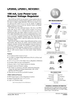
1 Semiconductor Components Industries, LLC, 2002 March, 2002 Rev. 01 Publication Order Number: 2N3819 /D2N3819 jfet VHF/UHF AmplifierN Channel DepletionMAXIMUM RATINGSR atingSymbolValueUnitDrain Source VoltageVDS25 VdcDrain Gate VoltageVDG25 VdcGate Source VoltageVGS25 VdcDrain CurrentID100mAdcForward Gate CurrentIG(f)10mAdcTotal Device Dissipation@ TA = 25 CDerate above 25 CStorage Channel Temperature RangeTstg 65 to +150 CDevicePackageShippingORDERING INFORMATION2N3819TO 92TO 92 CASE 29 STYLE 225000 Units/Box3212N3819 = Device CodeY= YearWW= Work WeekMARKING DIAGRAM2N3819 DRAIN1 SOURCE2 GATE2N3819 CHARACTERISTICS (TA = 25 C unless otherwise noted)CharacteristicSymbolMinTypMaxUnitO FF CHARACTERISTICSGate Source Breakdown Voltage(IG = Adc, VDS = 0)V(BR)GSS25 VdcGate Source(VDS = 15 Vdc, ID = 200 Adc) Source Cutoff Voltage(VDS = 15 Vdc, ID = 10 nAdc)VGS(off)
2 Reverse Current(VGS = 15 Vdc, VDS = 0)IGSS 210nAdcON CHARACTERISTICSZero Gate Voltage Drain Current(VDS = 15 Vdc, VGS = 0) 20mAdcSMALL SIGNAL CHARACTERISTICSF orward Transfer Admittance(VDS = 15 Vdc, VGS = 0, f = kHz) Yfs Admittance(VDS = 15 Vdc, VGS = 0, f = kHz) Yos 40 mhosForward Transfer Admittance(VDS = 15 Vdc, VGS = 0, f = 200 MHz) Yfs mmhosReverse Transfer Admittance(VDS = 15 Vdc, VGS = 0, f = 200 MHz) Yrs mmhosInput Capacitance(VDS = 20 Vdc, VGS = Vdc)Ciss pFReverse Transfer Capacitance(VDS = 20 Vdc, VGS = Vdc, f = MHz)Crss pFOutput Capacitance(VDS = 20 Vdc, VGS = Vdc, f = MHz)Coss pFCut off Frequency (Note 1)(VDS = 15 Vdc, VGS = 0)F(Yfs) 700 MHz1. The frequency at which gfs is of its value at 1 , FREQUENCY (MHz)3010bis @ IDSSf, FREQUENCY (MHz) 1.
3 Input Admittance (yis)Figure 2. Reverse Transfer Admittance (yrs)COMMON SOURCE CHARACTERISTICSADMITTANCE PARAMETERS(VDS = 15 Vdc, Tchannel = 25 C)f, FREQUENCY (MHz)20f, FREQUENCY (MHz)10 Figure 3. Forward Transadmittance (yfs)Figure 4. Output Admittance (yos)gis, INPUT CONDUCTANCE (mmhos) 70 100200300500 7001000bis, INPUT SUSCEPTANCE (mmhos)gfs, FORWARD TRANSCONDUCTANCE (mmhos)|bfs|, FORWARD SUSCEPTANCE (mmhos)grs, REVERSE TRANSADMITTANCE (mmhos)brs, REVERSE SUSCEPTANCE (mmhos) , OUTPUT ADMITTANCE (mhos)bos, OUTPUT SUSCEPTANCE (mhos) 700100010203050 70 100200 300500 70100200 300500 7001000bis @ IDSSgis @ IDSSgis @ IDSSbrs @ IDSSgrs @ IDSS, IDSSgfs @ IDSS|bfs| @ IDSS|bfs| @ IDSSbos @ IDSS and IDSSgos @ IDSSgos @ IDSSgfs @ IDSS2N3819 5. S11sFigure 6.
4 S12s0 350 340 330 10 20 30 180 190 200 210 170 160 150 323130292827262524232240 50 60 70 80 90 100 110 120 130 140 0 350 340 330 10 20 30 180 190 200 210 170 160 150 320 310 300 290 280 270 260 250 240 230 220 40 50 60 70 80 90 100 110 120 130 140 0 350 340 330 10 20 30 180 190 200 210 170 160 150 323130292827262524232240 50 60 70 80 90 100 110 120 130 140 0 350 340 330 10 20 30 180 190 200 210 170 160 150 320 310 300 290 280 270 260 250 240 230 220 40 50 60 70 80 90 100 110 120 130 140 = IDSSID = IDSS100200300400600700800900500ID = IDSS, IDSS900500800700600500400300200100ID = IDSSID = IDSS100200300400900600700800900800600400 300200200100ID = IDSSID = IDSS900100500700300400500600700800 Figure 7. S21sFigure 8. S22sCOMMON SOURCE CHARACTERISTICS S PARAMETERS(VDS = 15 Vdc, Tchannel = 25 C, Data Points in MHz) 2N3819 , FREQUENCY (MHz)10gig @ IDSSf, FREQUENCY (MHz) 9.
5 Input Admittance (yig)Figure 10. Reverse Transfer Admittance (yrg)COMMON GATE CHARACTERISTICSADMITTANCE PARAMETERS(VDG = 15 Vdc, Tchannel = 25 C)f, FREQUENCY (MHz)f, FREQUENCY (MHz)Figure 11. Forward Transfer Admittance (yfg)Figure 12. Output Admittance (yog)gig, INPUT CONDUCTANCE (mmhos) 70 100200300500 7001000big, INPUT SUSCEPTANCE (mmhos)gfg, FORWARD TRANSCONDUCTANCE (mmhos)bfg, FORWARD SUSCEPTANCE (mmhos)grg, REVERSE TRANSADMITTANCE (mmhos)brg, REVERSE SUSCEPTANCE (mmhos) , OUTPUT ADMITTANCE (mmhos)bog, OUTPUT SUSCEPTANCE (mmhos) 70010001020305070 100200 300500 100200 300500 7001000big @ IDSSbig @ IDSSgrg @ IDSSgfg @ IDSSgfg @ IDSSbrg @ IDSSbog @ IDSS, IDSSgog @ IDSSgog @ @ IDSSgig @ IDSS, IDSSbfg @ IDSS2N3819 350 340 330 10 20 30 180 190 200 210 170 160 150 320 310 300 290 280 270 260 250 240 230 220 40 50 60 70 80 90 100 110 120 130 140 0 350 340 330 10 20 30 180 190 200 210 170 160 150 323130292827262524232240 50 60 70 80 90 100 110 120 130 140 0 350 340 330 10 20 30 180 190 200 210 170 160 150 320 310 300 290 280 270 260 250 240 230 220 40 50 60 70 80 90 100 110 120 130 140 0 350 340 330 10 20 30 180 190 200 210 170 160 150 323130292827262524232240 50 60 70 80 90 100 110 120 130 140 Figure 13.
6 S11gFigure 14. S12gFigure 15. S21gFigure 16. = IDSSID = IDSS100200300400500600700800900900600700 800ID = IDSSID = IDSS100900100900ID = IDSSID = = IDSS, IDSSCOMMON GATE CHARACTERISTICS S PARAMETERS(VDS = 15 Vdc, Tchannel = 25 C, Data Points in MHz) 2N3819 DIMENSIONSCASE 29 11 ISSUE ALTO 92 (TO 226)NOTES:1. DIMENSIONING AND TOLERANCING PER , CONTROLLING DIMENSION: CONTOUR OF PACKAGE BEYOND DIMENSION RIS LEAD DIMENSION IS UNCONTROLLED IN P ANDBEYOND DIMENSION K X XCVDNNXXSEATINGPLANEDIM MINMAXMIN 22:PIN 1. SOURCE2. GATE3. DRAIN2N3819 Semiconductor is a trademark and is a registered trademark of Semiconductor Components Industries, LLC (SCILLC). SCILLC reserves the rightto make changes without further notice to any products herein.
7 SCILLC makes no warranty, representation or guarantee regarding the suitability of its productsfor any particular purpose, nor does SCILLC assume any liability arising out of the application or use of any product or circuit, and specifically disclaims anyand all liability, including without limitation special, consequential or incidental damages. Typical parameters which may be provided in SCILLC data sheetsand/or specifications can and do vary in different applications and actual performance may vary over time. All operating parameters, including Typicals mustbe validated for each customer application by customer s technical experts. SCILLC does not convey any license under its patent rights nor the rights of products are not designed, intended, or authorized for use as components in systems intended for surgical implant into the body, or other applicationsintended to support or sustain life, or for any other application in which the failure of the SCILLC product could create a situation where personal injury or deathmay occur.
8 Should Buyer purchase or use SCILLC products for any such unintended or unauthorized application, Buyer shall indemnify and hold SCILLCand its officers, employees, subsidiaries, affiliates, and distributors harmless against all claims, costs, damages, and expenses, and reasonable attorney feesarising out of, directly or indirectly, any claim of personal injury or death associated with such unintended or unauthorized use, even if such claim alleges thatSCILLC was negligent regarding the design or manufacture of the part. SCILLC is an Equal Opportunity/Affirmative Action ORDERING INFORMATIONJAPAN: ON Semiconductor , Japan Customer Focus Center4 32 1 Nishi Gotanda, Shinagawa ku, Tokyo, Japan 141 0031 Phone: 81 3 5740 2700 Email: Semiconductor Website: additional information, please contact your localSales Fulfillment:Literature Distribution Center for ON Box 5163, Denver, Colorado 80217 USAP hone: 303 675 2175 or 800 344 3860 Toll Free USA/CanadaFax: 303 675 2176 or 800 344 3867 Toll Free USA/CanadaEmail: American Technical Support: 800 282 9855 Toll Free USA/Canada
