Transcription of ADTL082/ADTL084 Low Cost JFET Input Operational …
1 Low Cost jfet InputOperational Amplifiers ADTL082/ADTL084 Rev. B Information furnished by analog devices is believed to be accurate and reliable. However, no responsibility is assumed by analog devices for its use, nor for any infringements of patents or other rights of third parties that may result from its use. Specifications subject to change without notice. No license is granted by implication or otherwise under any patent or patent rights of analog devices . Trademarks and registered trademarks are the property of their respective owners. One Technology Way, Box 9106, Norwood, MA 02062-9106, : Fax: 2007 analog devices , Inc.
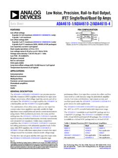
2 All rights reserved. FEATURES TL082/TL084 compatible Low Input bias current: 10 pA maximum Offset voltage mV maximum (ADTL082A/ADTL084A) 9 mV maximum (ADTL082J/ADTL084J) 15 V operation Low noise: 16 nV/ Hz Wide bandwidth: 5 MHz Slew rate: 20 V/ s CMRR: 80 dB minimum Total harmonic distortion: Supply current: mA typical Unity-gain stable APPLICATIONS General-purpose amplification Power control and monitoring Active filters Industrial/process control Data acquisition Sample and hold circuits Integrators Input buffering PIN CONFIGURATIONS OUT A1 IN A2+IN A3 V4+V8 OUT B7 IN B6+IN B5 adtl082 JTOP VIEW(Not to Scale)06275-001 Figure 1.
3 8-Lead SOIC_N (R-8) OUT A1 IN A2+IN A3 V4+V8 OUT B7 IN B6+IN B5 adtl082 ATOP VIEW(Not to Scale)06275-002 Figure 2. 8-Lead MSOP (RM-8) OUT A1 IN A2+IN A3+V4 OUT D14 IN D13+IN D12 V11+IN B5+IN C10 IN B6 IN C9 OUT B7 OUT C8 ADTL084 JTOP VIEW(Not to Scale)06275-003 Figure 3. 14-Lead SOIC_N (R-14) ADTL084A1234567 IN A+IN A+VOUT B IN B+IN BOUT A141312111098 IN D+IN D VOUT C IN C+IN COUT DTOP VIEW(Not to Scale)06275-004 Figure 4. 14-Lead TSSOP (RU-14) GENERAL DESCRIPTION The adtl082 and ADTL084 are jfet Input amplifiers that provide industry-leading performance over TL08x devices . The ADTL082A and ADTL084A are improved versions of TL08x A, I, and Q grades.
4 The ADTL082J and ADTL084J are industry alternatives to the TL08x standard and C grades. The ADTL08x family offers lower noise, offset voltage, offset drift over temperature, and bias current over the TL08x. In addition, the ADLT08x family has better common-mode rejection and slew rates. These op amps are ideal for various applications, including process control, industrial and instrumentation equipment, active filtering, data conversion, buffering, and power control and monitoring. The A grade amplifiers are available in lead-free packaging. The standard grade amplifiers are available in both leaded and lead-free packaging.
5 The ADTL082A and ADTL084A are specified over the extended industrial ( 40 C to +125 C) temperature range. The ADTL082J and ADTL084J are specified over the commercial (0 C to 70 C) temperature range. ADTL082/ADTL084 Rev. B | Page 2 of 12 TABLE OF CONTENTS 1 1 Pin 1 General 1 Revision 2 3 Absolute Maximum 4 Thermal Power ESD Ty pi c a l Pe r f o r m a n c e C h a r a c t e r i s t i c Outline Ordering 10 REVISION HISTORY 11/07 Rev. A to Rev. B Changes to Ordering Guide .. 10 4/07 Rev. 0 to Rev. A Changes to Table 3 1/07 Revision 0: Initial Version ADTL082/ADTL084 Rev.
6 B | Page 3 of 12 SPECIFICATIONS VCC = 15 V, VCM = 0 V, TA = 25 C, over all grades, unless otherwise noted. Table 1. J Grade A Grade Parameter Symbol Conditions Min Typ Max Min Typ Max Unit Input CHARACTERISTICS Offset Voltage VOS 2 9 mV 0 C
7 TA +70 C 10 8 mV 40 C TA +125 C 9 mV Offset Voltage Drift VOS/ T 0 C TA +70 C 15 V/ C 40 C TA +125 C 10 V/ C Input Bias Current IB 2 100 2 100 pA 0 C TA +70 C 3 3 nA
8 40 C TA +125 C 5 nA Input Offset Current IOS 2 100 2 100 pA 0 C TA 70 C 3 3 nA 40 C TA +125 C 5 nA Input Voltage Range VCM 11 +15 11 +15 V Common-Mode Rejection Ratio CMRR VCM = 11 V to +15 V 80 86 80
9 86 dB Input Impedance RIN 1012 1012 Large Signal Voltage Gain AVORL = 2 k , VO = 10 V to +10 V 100 200 100 200 V/mV 0 C TA 70 C 90 200 90 200 V/mV 40 C
10 TA +125 C 50 200 V/mV OUTPUT CHARACTERISTICS Maximum Output Voltage Swing VORL = 10 k 12 13 V 0 C TA +70 C 12 13 V 40 C TA +125 C 13 V RL = 2 k V