Transcription of AD8610/AD8620 Precision, Very Low Noise, Low Input Bias ...
1 precision , Very Low Noise, Low Input Bias Current, Wide Bandwidth jfet Operational Amplifiers AD8610/AD8620 Rev. F Information furnished by Analog Devices is believed to be accurate and reliable. However, no responsibility is assumed by Analog Devices for its use, nor for any infringements of patents or other rights of third parties that may result from its use. Specifications subject to change without notice. No license is granted by implication or otherwise under any patent or patent rights of Analog Devices. Trademarks and registered trademarks are the property of their respective owners.
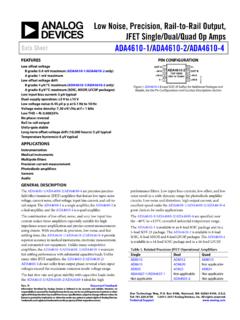
2 One Technology Way, Box 9106, Norwood, MA 02062-9106, : Fax: 2001 2008 Analog Devices, Inc. All rights reserved. FEATURES Low noise: 6 nV/ Hz Low offset voltage: 100 V maximum Low Input bias current: 10 pA maximum Fast settling: 600 ns to Low distortion Unity gain stable No phase reversal Dual-supply operation: 5 V to 13 V APPLICATIONS Photodiode amplifiers AT E Instrumentation Sensors and controls High performance filters Fast precision integrators High performance audio PIN CONFIGURATIONS NC = NO CONNECTAD8610 TOP VIEW(Not to Scale)NULL1 IN2+IN3V 4 NCV+OUTNULL876502730-001 Figure 1. 8-Lead MSOP and 8-Lead SOIC_N AD8620 TOP VIEW(Not to Scale)OUTA1 INA2+INA3V 4V+OUTB INB+INB02730-0028765 Figure 2.
3 8-Lead SOIC_N GENERAL DESCRIPTIONThe AD8610/AD8620 are very high precision jfet Input ampli- fiers featuring ultralow offset voltage and drift, very low Input voltage and current noise, very low Input bias current, and wide bandwidth. Unlike many jfet amplifiers, the AD8610/AD8620 Input bias current is low over the entire operating temperature range. The AD8610/AD8620 are stable with capacitive loads of over 1000 pF in noninverting unity gain; much larger capacitive loads can be driven easily at higher noise gains. The AD8610/ AD8620 swing to within V of the supplies even with a 1 k load, maximizing dynamic range even with limited supply volt-ages.
4 Outputs slew at 50 V/ s in either inverting or noninverting gain configurations, and settle to accuracy in less than 600 ns. Combined with high Input impedance, great precision , and very high output drive, the AD8610/AD8620 are ideal amplifiers for driving high performance ADC inputs and buffering DAC converter outputs. Applications for the AD8610/AD8620 include electronic instru-ments; ATE amplification, buffering, and integrator circuits; CAT/MRI/ultrasound medical instrumentation; instrumentation quality photodiode amplification; fast precision filters (including PLL filters); and high quality audio. The AD8610/AD8620 are fully specified over the extended industrial temperature range ( 40 C to +125 C).
5 The AD8610 is available in the narrow 8-lead SOIC and the tiny 8-lead MSOP surface-mount packages. The AD8620 is available in the narrow 8-lead SOIC package. The 8-lead MSOP packaged devices are avail-able only in tape and reel. AD8610/AD8620 Rev. F | Page 2 of 24 TABLE OF CONTENTS Features .. 1 Applications .. 1 Pin Configurations .. 1 General Description .. 1 Revision History .. 2 Specifications .. 3 Electrical Specifications .. 4 Absolute Maximum Ratings ..5 ESD Typical Performance Characteristics ..6 Theory of Operation .. 13 Functional Description .. 13 Outline Dimensions .. 22 Ordering Guide .. 22 REVISION HISTORY 5/08 Rev.
6 E to Rev. F Changes to Figure 17 .. 8 Changes to Functional Description Section .. 13 Changes to THD Readings vs. Common-Mode Voltage Section .. 17 Changes to Output Current Capability Section .. 18 Changes to Figure 66 and Figure 67 .. 19 Changes to Figure 68 .. 20 Replaced Second-Order Low-Pass Filter Section .. 20 11/06 Rev. D to Rev. E Updated Format .. Universal Changes to Table 1 .. 3 Changes to Table 2 .. 4 Changes to Outline Dimensions .. 21 Changes to Ordering Guide .. 21 2/04 Rev. C to Rev. D. Changes to Specifications .. 2 Changes to Ordering Guide .. 4 Updated Outline Dimensions .. 17 10/02 Rev. B to Rev.
7 C. Updated Ordering Guide .. 4 Edits to Figure 15 .. 12 Updated Outline Dimensions .. 16 5/02 Rev. A to Rev. B Addition of Part Number AD8620 .. Universal Addition of 8-Lead SOIC (R-8 Suffix) Drawing .. 1 Changes to General Description .. 1 Additions to Specifications .. 2 Change to Electrical Specifications .. 3 Additions to Ordering Guide .. 4 Replace TPC 29 .. 8 Add Channel Separation Test Circuit Figure .. 9 Add Channel Separation Graph .. 9 Changes to Figure 26 .. 15 Addition of High-Speed, Low Noise Differential Driver section .. 16 Addition of Figure 30 .. 16 AD8610/AD8620 Rev. F | Page 3 of 24 SPECIFICATIONS @ VS = V, VCM = 0 V, TA = 25 C, unless otherwise noted.
8 Table 1. Parameter Symbol Conditions Min Typ Max Unit Input CHARACTERISTICS Offset Voltage (AD8610B) VOS 45 100 V 40 C < TA < +125 C 80 200 V Offset Voltage (AD8620B)
9 VOS 45 150 V 40 C < TA < +125 C 80 300 V Offset Voltage (AD8610A/AD8620A) VOS 85 250 V 25 C < TA < 125 C 90 350 V 40 C
10 < TA < +125 C 150 850 V Input Bias Current IB 10 +2 +10 pA 40 C < TA < +85 C 250 +130 +250 pA 40 C < TA < +125 C + + nA Input Offset Current IOS 10 +1 +10 pA