Transcription of Low noise JFET single operational amplifier
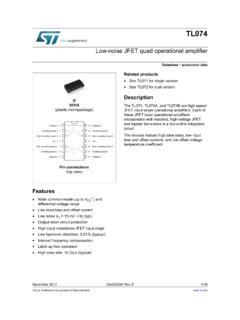
1 September 2008 Rev 31/1515TL071 Low noise jfet single operational amplifierFeatures Wide common-mode (up to VCC+) and differential voltage range Low input bias and offset currenT Low noise en = 15 nV/ Hz (typ) Output short-circuit protection High input impedance jfet input stage Low harmonic distortion: % (typ) Internal frequency compensation Latch-up free operation High slew rate: 16 V / s (typ)DescriptionThe TL071 is a high-speed jfet input single operational amplifier . This jfet input operational amplifier incorporates well matched, high-voltage jfet and bipolar transistors in a monolithic integrated device features high slew rates, low input bias and offset currents, and low offset voltage temperature (Plastic package)DSO-8(Plastic micropackage)123486571 - Offset null 12 - Inverting input3 - Non-inverting input4 - VCC- 5 - Offset null 26 - Output7 - VCC+8 - connections(Top view)
2 DiagramTL0712/15 1 Schematic diagramFigure schematicsFigure offset voltage null circuitOutputNon-invertinginputInverting inputVCCVCC100 Null1 Offset Null2100 200 N1N2TL071100k VCCTL071 Absolute maximum ratings and operating conditions 3/152 Absolute maximum ratings and operating conditions Table maximum ratingsSymbolParameterValueUnitTL071M, AM, BM TL071I, AI, BITL071C, AC, BCVCCS upply voltage (1) 18 VViInput voltage (2) 15 VVidDifferential input voltage (3) 30 VRthjaThermal resistance junction to ambient(4) (5)SO-8 DIP812585 C/WRthjcThermal resistance junction to case(4) (5)SO-8 DIP84041 C/WOutput short-circuit duration (6)InfiniteToperOperating free-air temperature range-55 to +125-40 to +1050 to +70 CTstgStorage temperature range-65 to +150 CESDHBM: human body model(7)500 VMM: machine model(8)200 VCDM: charged device model(9)1500V1.
3 All voltage values, except differential voltage, are with respect to the zero reference level (ground) of the supply voltages where the zero reference level is the midpoint between VCC+ and The magnitude of the input voltage must never exceed the magnitude of the supply voltage or 15 volts, whichever is Differential voltages are the non-inverting input terminal with respect to the inverting input Short-circuits can cause excessive heating. Destructive dissipation can result from simultaneous short-circuits on all Rth are typical The output may be shorted to ground or to either supply. Temperature and/or supply voltages must be limited to ensure that the dissipation rating is not Human body model: 100 pF discharged through a k resistor between two pins of the device, done for all couples of pin combinations with other pins floating.
4 8. Machine model: a 200 pF cap is charged to the specified voltage, then discharged directly between two pins of the device with no external series resistor (internal resistor < 5 ), done for all couples of pin combinations with other pins Charged device model: all pins plus package are charged together to the specified voltage and then discharged directly to the conditionsSymbolParameterTL071I, AI, BITL071C, AC, BCUnitVCCS upply voltage6 to 36 VToperOperating free-air temperature range-40 to +1050 to +70 CElectrical characteristicsTL0714/15 3 Electrical characteristics Table = 15V, Tamb = +25 C (unless otherwise specified)SymbolParameterTL071I,M,AC,AI, AM,BC,BI, offset voltage (Rs = 50 )
5 Tamb = +25 CTL071TL071 ATL071 BTmin Tamb TmaxTL071TL071 ATL071B3311063137531013mVDVioInput offset voltage drift1010 V/ CIioInput offset current Tamb = +25 CTmin Tamb Tmax51004510010pAnAIibInput bias current (1)Tamb = +25 CTmin Tamb Tmax20200202020020pAnAAvdLarge signal voltage gain (RL= 2k , Vo= 10V) Tamb = +25 CTmin Tamb Tmax50252002515200V/mVSVRS upply voltage rejection ratio (RS = 50 )Tamb = +25 CTmin Tamb Tmax808086707086dBICCS upply current, no load Tamb = +25 CTmin Tamb common mode voltage range 11+15-12 11+15-12 VCMRC ommon mode rejection ratio (RS = 50 )Tamb = +25 CTmin Tamb Tmax808086707086dBIosOutput short-circuit currentTamb = +25 CTmin Tamb Tmax10104060601010406060mA VoppOutput voltage swing Tamb = +25 C RL = 2k RL = 10k Tmin Tamb Tmax RL = 2k RL = 10k rateVin = 10V, RL = 2k , CL = 100pF, unity gain816816V/ sTL071 Electrical characteristics 5/15trRise time Vin = 20mV, RL = 2k , CL = 100pF, unity sKovOvershoot Vin = 20mV, RL = 2k , CL = 100pF, unity gain1010%GBPGain bandwidth product Vin = 10mV, RL = 2k , CL = 100pF.
6 F= resistance10121012 WTHDT otal harmonic distortion, f= 1kHz, RL= 2k ,CL = 100pF, Av = 20dB,Vo = 2 Vpp) input noise voltageRS = 100 , f = 1 KHz1515 mPhase margin4545degrees1. The input bias currents are junction leakage currents which approximately double for every 10 C increase in the junction = 15V, Tamb = +25 C (unless otherwise specified) (continued)SymbolParameterTL071I,M,AC,AI ,AM,BC,BI, characteristicsTL0716/15 Figure peak-to-peak output voltage versus frequencyFigure peak-to-peak output voltage versus frequency Figure peak-to-peak output voltage versus frequencyFigure peak-to-peak output voltage versus free air temp.
7 Figure peak-to-peak output voltage versus load resistanceFigure peak-to-peak output voltage versus supply voltage 302520151050246810121416M AXIMUM PEAK-TO-PEAK OUTPUTVOLTAGE (V)RL= 10 k Tamb= +25 CSUPPLY VOLTAGE ( V)TL071 Electrical characteristics 7/15 Figure bias current versus free air temperatureFigure 10. Large signal differential voltage amplification versus free air temp. BIAS CURRENT (nA)-50-250255075100125 TEMPERATURE ( C)VCC=15V1000400200100204010421 DIFFERENTIAL VOLTAGE AMPLIFICATION (V/V)-75-50-250255075100125 TEMPERATURE ( C)RL= 2k VO= 10 VVCC= 15 VFigure 11.
8 Large signal differential voltage amplification and phase shift versus frequencyFigure 12. Total power dissipation versus free air temperature FREQUENCY (Hz)DIFFERENTIAL VOLTAGEAMPLIFICATION (V/V)100101001K10K100K10M1M1 DIFFERENTIAL VOLTAGEAMPLIFICATION(left scale)180900R = 2kWC = 100pFV = 15VT = +125 CLLCCambPHASE SHIFT(right scale)2502252001751501251007550250 TOTAL POWER DISSIPATION (mW)-75-50-250255075100125 TEMPERATURE ( C)VCC= 15 VNo signalNo loadFigure 13. Supply current per amplifier versus free air temperatureFigure 14. Common mode rejection ratio versus free air temperature CURRENT (mA)-75-50-250255075100125 TEMPERATURE ( C)VCC= 15 VNo signalNo load898887868584-50-250255075100125 COMMON MODE MODE REJECTIONRATIO (dB)TEMPERATURE ( C)83-75RL= 10 k = 15 VVCCE lectrical characteristicsTL0718/15 Parameter measurement information Figure 15.
9 Voltage follower large signal pulse responseFigure 16. Output voltage versus elapsed time AND OUTPUT VOLTAGES(V)TIME (ms)-6= 15 VVCCRL= 2 kW= 100pFCLTamb= +25 COUTPUTINPUTtr2824201612840-4 OUTPUT VOLTAGE (mV) ( s)10%90%OVERSHOOTRL= 2k Tamb= +25 CVCC= 15 VFigure 17. Equivalent input noise voltage versus frequencyFigure 18. Total harmonic distortion versus frequency 706050403020100 EQUIVALENT input NOISEVOLTAGE (nV/VHz)10401004001k4k10k40k 100kFREQUENCY (Hz)AV= 10RS= 100 Tamb= +25 CVCC= HARMONIC DISTORTION(%)1004001k4k10k40k100kFREQUEN CY (Hz)AV= 1 Tamb= +25 CVCC= 15V= 6 VVO(rms)AV= 1 Tamb= +25 C= 6 VVO(rms)VCC= 15 VFigure 19.
10 Voltage followerFigure 20. Gain-of-10 inverting amplifier --eITL071eoCL= 100pFR = 2k L-eITL071 RLCL= 100pF1k 10k eoTL071 Typical applications 9/154 Typical applicationsFigure 21. ( Hz) Square wave oscillatorFigure 22. High Q notch filter-TL0 711k RF= 100k + C = FFf = osc1F2 x RFCTL071-R1R2C3R3C2C1C1 = C2 =C32= 100pFf = o1F2 x RFC= 1kHzR1 = R2 = 2R3 = Package informationTL07110/15 5 Package informationIn order to meet environmental requirements, STMicroelectronics offers these devices in ECOPACK packages.