Transcription of Junction Field Effect Transistor (JFET)
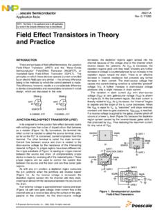
1 Junction Field Effect Transistor ( jfet ) The single channel Junction Field - Effect Transistor ( jfet ) is probably the simplest Transistor available. As shown in the schematics below (Figure in your text) for the n-channel jfet (left) and the p-channel jfet (right), these devices are simply an area of doped silicon with two diffusions of the opposite doping. Please be aware that the schematics presented are for illustrative purposes only and are simplified versions of the actual device. Note that the material that serves as the foundation of the device defines the channel type. Like the BJT, the jfet is a three terminal device. Although there are physically two gate diffusions, they are tied together and act as a single gate terminal.
2 The other two contacts, the drain and source, are placed at either end of the channel region. The jfet is a symmetric device (the source and drain may be interchanged), however it is useful in circuit design to designate the terminals as shown in the circuit symbols above. The operation of the jfet is based on controlling the bias on the pn Junction between gate and channel (note that a single pn Junction is discussed since the two gate contacts are tied together in parallel what happens at one gate-channel pn Junction is happening on the other). If a voltage is applied between the drain and source, current will flow (the conventional direction for current flow is from the terminal designated to be the gate to that which is designated as the source). The device is therefore in a normally on state.
3 To turn it off, we must apply an appropriate voltage to the gate and use the depletion region created at the Junction to control the channel width. The following discussion is going to focus on the n-channel jfet (analogous to the npn BJT). The operating and characteristics of the p-channel jfet may then be deduced by making the necessary changes to voltage polarities and current directions. The following definitions and conditions will hold throughout our analysis: The source of the jfet will provide a common ground for all device terminals. While this is not required, it is common practice. The voltage applied to the drain will be designated vDD. Note that in some other texts and literature this is referred to as vDS. The voltage applied to the gate will be designated vGG.
4 Note that in some other texts and literature this is referred to as vGS. The n-channel jfet connected to the voltages sources vDD and vGG is presented to the right (Figure of your text). The polarity indicated for vDD means that the electrons in the channel will be attracted to the drain and conventional current will flow in the direction indicated by iD (remember that negative charges moving in a negative direction have the same Effect as positive charges moving in a positive direction). The polarity voltage applied to the gate (vGG) ensures that the gate-channel pn Junction will be reverse biased and essentially no current will flow (the reverse bias saturation current is considered negligible). The jfet is a voltage-controlled device, with two controlling voltages (vDD and vGG).
5 We are going to look at these individually and then combine the results for the overall jfet characteristics. jfet Drain-To-Source Voltage Variation To follow the development in your text, the first Effect we re going to look at is the variation of the drain-to-source voltage through the applied voltage vDD. The figure to the right is a modified version of Figure in your text. For purposes of this discussion, the gate-to-source voltage is zero, although the same will hold true for any suitable vGG (hang on, that part is coming up next). Anyway, please bear with my attempt at artwork as we go through this! For a constant vGG, the Effect of vDD variation may be illustrated as follows: vDD must be greater than zero for current to flow in the direction defined in an n-channel jfet .
6 The applied vDD, or the voltage between drain and source (ground) appears as a voltage drop across the length of the channel, with the voltage increasing along the channel from source to drain ( , vDS=0 at the source, vDS=vDD at the drain). We re also going to assume a constant doping so that the voltage variation in the channel is linear (vGG also affects this talked about below). When vDD is very small, the voltage variation in the channel is very small and it has no Effect on the channel shape. For this case, the depletion region is only due to the pn Junction as shown in yellow in the figure. As vDD increases, the increasing potential at the drain reverse biases the pn junctions. Since the voltage drop across the channel increases from source to drain, the reverse bias of the pn Junction also increases from source to drain.
7 Since the depletion region is a function of bias, the depletion region also gets wider from source to drain, causing the channel to become tapered as shown in red in the figure. The current still increases with increasing vDD, however there is no longer a linear relationship between vDD and iD since the channel resistance is a function of its width. Further increases in vDD, for example, blue in the figure, result in a more tapered shape to the channel and increasing nonlinearities in the iD-vDD relationship. This process continues until a vDS is reached where the depletion regions from the pn junctions merge. Analytically, this occurs when the gate-to-drain voltage vGD is less than some threshold VP (note that some sources denote the threshold as VT) and is known as the pinch-off point.
8 At this point, the drain current saturates and further increases in vDS result in little (ideally zero) change in iD. For the case vGG=vGS=0, the drain current at pinch-off is called the drain-source saturation current, IDSS. Operation beyond the pinch-off point (vDS > vGS VP for an n-channel device) defines the normal operating or saturation region of the jfet . jfet Gate-To-Source Voltage Variation For a constant vGG, varying vDS yields a single iD-vDS characteristic curve. To develop a family of characteristic curves for the jfet device, we need to look at the Effect of vGS variation. The figure to the right is a simple illustration of the variation of vGG with a constant (and small) vDD.
9 Recall from the previous discussion that, if vDD is small, vDS is small and the channel width is essentially constant. In the figure, the increasing width of the pn Junction depletion region (illustrated from yellow to red to blue), is due to the increasing reverse bias of the Junction resulting from the application of a negative vGG of increasing magnitude. As the depletion widths increase, the channel width decreases, resulting in a lower conductivity (higher resistivity) of the channel. As vGS is made more negative (for an n-channel device), a value of vGS is reached for which the channel is completely depleted (no free carriers) and no current will flow regardless of the applied vDS. This is called the threshold, or pinch-off, voltage and occurs at vGS=VGS(OFF).
10 The threshold voltage for an n-channel jfet is negative (VP < 0, using your text s notation). If we now apply the vDS variation Effect , we can see that pinch-off will occur for lower values of vDS since we have less of a channel to start with (resulting in lower values of iD at pinch-off). By combining the Effect of vDS and vGS variations, a family of characteristic curves similar to the figure at the right (based on Figure of your text) will be generated for the n-channel jfet . Similar results are illustrated in the family of characteristic curves presented to the right, and may be obtained for a p-channel jfet by following the previous discussion with the following modifications: The polarity of vDS is switched since the majority carriers are holes.