Transcription of 5.11 THE JUNCTION FIELD-EFFECT TRANSISTOR (JFET)
1 JFETs, GaAs DEVICES AND CIRCUITS, AND TTL CIRCUITS 1 JUNCTION FIELD-EFFECT TRANSISTOR ( jfet ) The JUNCTION FIELD-EFFECT TRANSISTOR , or jfet , is perhaps the simplest TRANSISTOR available. Ithas some important characteristics, notably a very high input resistance. Unfortunately,however (for the jfet ), the MOSFET has an even higher input resistance. This, togetherwith the many other advantages of MOS transistors, has made the jfet virtually , its applications are limited to discrete-circuit design, where it is used both as anamplifier and as a switch. Its integrated-circuit applications are limited to the design of thedifferential input stage of some operational amplifiers, where advantage is taken of its highinput resistance (compared to the BJT).
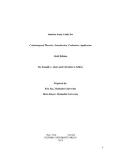
2 In this section, we briefly consider jfet operationand characteristics. Another important reason for including the jfet in the study of elec-tronics is that it helps in understanding the operation of gallium arsenide devices, the subjectof the next section. Device Structure As with other FET types, the jfet is available in two polarities: n -channel and p (a) shows a simplified structure of the n -channel jfet . It consists of a slabof n -type silicon with p -type regions diffused on its two sides. The n region is the chan-nel, and the p -type regions are electrically connected together and form the gate. Thedevice operation is based on reverse-biasing the pn JUNCTION between gate and , it is the reverse bias on this JUNCTION that is used to control the channel widthand hence the current flow from drain to source.
3 The major role that this pn junctionplays in the operation of this FET has given rise to its name: JUNCTION FIELD-EFFECT Tran- sistor ( jfet ). FIGURE (a) Basic structure of n -channel jfet . This is a simplified structure utilized to explaindevice operation. (b) Circuit symbol for the n -channel jfet . (c) Circuit symbol for the p -channel (a)(b)(c) 2010 Oxford University Press, Inc. Reprinting or distribution, electronically or otherwise, without the express written consent of Oxford University Press, Inc. is material is from a previous edition ofMicroelectronic Circuits. Thesesections provide valuable information, but please note that the references donot correspond to the 6th or 7th edition of the text.
4 2 MICROELECTRONIC CIRCUITSSEDRA/SMITH It should be obvious that a p -channel device can be fabricated by simply reversing all thesemiconductor types, thus using p -type silicon for the channel and n -type silicon for the (b) and (c) show the circuit symbols for JFETs of both polarities. Observethat the device polarity ( n -channel or p -channel) is indicated by the direction of the arrow-head on the gate line. This arrowhead points in the forward direction of the gate channel pn JUNCTION . Although the jfet is a symmetrical device whose source and drain can beinterchanged, it is useful in circuit design to designate one of these two terminals as sourceand the other as drain. The circuit symbol achieves this designation by placing the gatecloser to the source than to the drain.
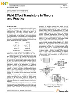
5 Physical Operation Consider an n -channel jfet and refer to Fig. (a). (Note that to simplify matters, wewill not show the electrical connection between the gate terminals; it is assumed, how-ever, that the two terminals labeled G are joined together.) With v GS = 0, the application ofa voltage v DS causes current to flow from the drain to the source. When a negative v GS isapplied, the depletion region of the gate channel JUNCTION widens and the channel be-comes correspondingly narrower; thus the channel resistance increases and the current i D (for a given v DS ) decreases. Because v DS is small, the channel is almost of uniformwidth. The jfet is simply operating as a resistance whose value is controlled by v GS.
6 Ifwe keep increasing v GS in the negative direction, a value is reached at which the depletionregion occupies the entire channel. At this value of v GS the channel is completely depletedof charge carriers (electrons); the channel has in effect disappeared. This value of v GS is therefore the threshold voltage of the device, V t , which is obviously negative for an n -channel jfet . For JFETs the threshold voltage is called the pinch-off voltage and isdenoted V P .Consider next the situation depicted in Fig. (b). Here v GS is held constant at a valuegreater (that is, less negative) than V P , and v DS is increased. Since v DS appears as a voltagedrop across the length of the channel, the voltage increases as we move along the channelfrom source to drain.
7 It follows that the reverse-bias voltage between gate and channel variesat different points along the channel and is highest at the drain end. Thus the channelacquires a tapered shape and the i D v DS characteristic becomes nonlinear. When the reversebias at the drain end, v GD , falls below the pinch-off voltage V P , the channel is pinched off atthe drain end and the drain current saturates. The remainder of the description of jfet oper-ation follows closely that given for the depletion description above clearly indicates that the jfet is a depletion-type device. Its char-acteristics should therefore be similar to those of the depletion-type MOSFET. This is truewith a very important exception: While it is possible to operate the depletion-type MOSFETin the enhancement mode (by simply applying a positive v GS if the device is n channel) thisis impossible in the jfet case.
8 If we attempt to apply a positive v GS , the gate channel pn JUNCTION becomes forward biased and the gate ceases to control the channel. Thus themaximum v GS is limited to 0 V, though it is possible to go as high as V or so since a pn JUNCTION remains essentially cut off at such a small forward voltage. Current Voltage Characteristics The current voltage characteristics of the jfet are identical to those of the depletion-modeMOSFET studied in Section except that for the jfet the maximum v GS allowed is 2010 Oxford University Press, Inc. Reprinting or distribution, electronically or otherwise, without the express written consent of Oxford University Press, Inc. is prohibited.
9 JFETs, GaAs DEVICES AND CIRCUITS, AND TTL CIRCUITS 3 normally 0 V. Furthermore, the jfet is specified in terms of the pinch-off voltage V P (equalto V t of the MOSFET) and the d rain-to- s ource current with the gate s horted to the source, I DSS , which corresponds to for the MOSFET. With these substitutions, the n -channelJFET characteristics can be described as follows:Cutoff: FIGURE Physical operation of the n -channel jfet : (a) F or small v DS the channel is uniform and thedevice functions as a resistance whose value is controlled by v GS . (b) Increasing v DS causes the channel toacquire a tapered shape and eventually pinch-off occurs. Note that, though not shown, the two gate regionsare electrically connected.
10 (a)(b)12---kn Vt2vGSVP, iD0= 2010 Oxford University Press, Inc. Reprinting or distribution, electronically or otherwise, without the express written consent of Oxford University Press, Inc. is prohibited. 4 MICROELECTRONIC CIRCUITSSEDRA/SMITH Triode region: ( )Saturation (pinch-off) region: ( )where is the inverse of the Early voltage; = 1 / V A , and V A and are positive for n -channel that for an n -channel device, V P is negative, we see that operation in thepinch-off region is obtained when the drain voltage is greater than the gate voltage by atleast | V P | . Since the gate channel JUNCTION is always reverse-biased, only a leakage current flowsthrough the gate terminal. From Chapter 3, we know that such a current is of the order of10 9 A.