Search results with tag "Effect transistor"

Bipolar Junction Transistor (BJT) Basics- GATE Problems
www.gatestudy.com(a) Bipolar junction transistors (b) NMOS transistors (c) Unipolar junction transistors (d) Junction field – effect transistors [GATE 1995] Soln. Ebers Moll model is one of classical models of BJT for small signals. This model is based on interacting diode junctions and is applicable to any transistor operating modes Option (a)
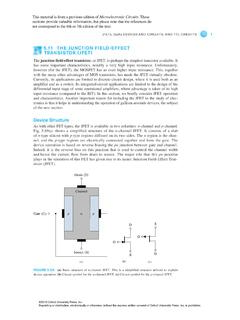
5.11 THE JUNCTION FIELD-EFFECT TRANSISTOR (JFET)
global.oup.com5.11 THE JUNCTION FIELD-EFFECT TRANSISTOR (JFET) The junction field-effect transistor, or JFET, is perhaps the simplest transistor available. It has some important characteristics, notably a very high input resistance. Unfortunately, however (for the JFET), the MOSFET has an even higher input resistance. This, together
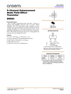
BSS84 - P-Channel Enhancement Mode Field-Effect Transistor
www.onsemi.comMode Field-Effect Transistor BSS84 General Description This P−channel enhancement−mode field−effect transistor is produced using onsemi’s proprietary, high cell density, DMOS technology. This very high density process minimizes on−state resistance and to provide rugged and reliable performance and fast switching.
11EDCField-effect transistorUnivMalasiya (FET)Lesson11.ppt
www.dauniv.ac.inThe Field Effect Transistor (FET) In 1945, Shockley had an idea for making a solid state device out of semiconductors. He reasoned that a strong electrical field could cause the flow of electricity within a nearby semiconductor. He tried to build one, but it didn't work. Three years later, Brattain & Bardeen built the first working transistor, the germanium point-contact

TEACHING SYLLABUS FOR PHYSICS (SENIOR HIGH SCHOOL)
scienceandtechclub.webs.comUnit 1 : Photoelectric effect and wave particle duality Unit 2 : Thermionic emission, cathode rays and x-rays Section 6 : Electronics(pg 46-47) Unit 1: Bipolar Junction Transistor (BJT) and Junction Field-Effect Transistor (JFET) Section 1: Motion, Forces and Energy (pg 48) Unit 1 : Rotational motion of solid objects

AOD4189 P-Channel Enhancement Mode Field Effect Transistor
aosmd.comSymbol VDS VGS IDM IAR EAR TJ, TSTG Symbol Typ Max 15 20 41 50 RθJC 2 2.4 °C 62.5 31-55 to 175 W 2.5 1.6 Continuous Drain Current B,H Parameter Maximum Units TC=25°C TC=100°C-40 Absolute Maximum Ratings TC=25°C unless otherwise noted V TA=70°C Power Dissipation B Avalanche Current C Repetitive avalanche energy L=0.1mH C A