Transcription of Wide bandwidth single JFET operational amplifiers
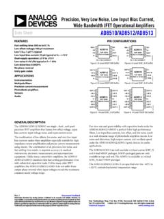
1 April 2008 Rev 21/1414LF351 Wide bandwidth single jfet operational amplifiersFeatures Internally adjustable input offset voltage Low power consumption Wide common-mode (up to VCC+) and differential voltage range Low input bias and offset current Output short-circuit protection High input impedance jfet input stage Internal frequency compensation Latch up free operation High slew rate 16 V/ s (typical)DescriptionThese circuits are high speed jfet input single operational amplifiers incorporating well matched, high voltage jfet and bipolar transistors in a monolithic integrated devices feature high slew rates, low input bias and offset currents, and low offset voltage temperature (Plastic package)DSO-8(Plastic micro package)123486571 - Offset null 12 - Inverting input3 - Non-inverting input4 - VCC- 5 - Offset null 26 - Output7 - VCC+ 8 - connections(top view)
2 1 SchematicsFigure diagramFigure offset voltage null circuit Null1 Offset Null2100W200 WLF351 Absolute maximum ratings and operating conditions 3/142 Absolute maximum ratings and operating conditions Table maximum ratingsSymbolParameterValueUnitVCCS upply voltage(1) 18 VViInput voltage(2) 15 VVidDifferential input voltage(3) 30 VRthjaThermal resistance junction to ambient(4)SO-8 DIP812585 C/WRthjcThermal resistance junction to case(4)SO-8 DIP84041 C/WOutput short-circuit duration(5)InfiniteTstgStorage temperature range-65 to +150 CESDHBM: human body model(6)500 VMM: machine model(7)200 VCDM: charged device model(8) All voltage values, except differential voltage, are with respect to the zero reference level (ground) of the supply voltages where the zero reference level is the midpoint between VCC+ and The magnitude of the input voltage must never exceed the magnitude of the supply voltage or 15 volts, whichever is Differential voltages are the non-inverting input terminal with respect to the inverting input Short-circuits can cause excessive heating and destructive dissipation.
3 Values are The output may be shorted to ground or to either supply. Temperature and/or supply voltages must be limited to ensure that the dissipation rating is not exceeded6. Human body model: A 100 pF capacitor is charged to the specified voltage, then discharged through a k resistor between two pins of the device. This is done for all couples of connected pin combinations while the other pins are floating. 7. Machine model: A 200 pF capacitor is charged to the specified voltage, then discharged directly between two pins of the device with no external series resistor (internal resistor < 5 ). This is done for all couples of connected pin combinations while the other pins are Charged device model: all pins and the package are charged together to the specified voltage and then discharged directly to the ground through only one pin.
4 This is done for all conditionsSymbolParameterLF151LF251LF351 UnitVCCS upply voltage6 to 32 VToperOperating free-air temperature range-55 to +125-40 to +1050 to +70 CElectrical characteristicsLF3514/14 3 Electrical characteristics Table characteristics at VCC = 15 V, Tamb = +25 C (unless otherwise specified)SymbolParameterMin. Typ. offset voltage (Rs = 10k ) Tmin Tamb Tmax31013mVDVioInput offset voltage drift10 V/ CIioInput offset current (1) Tmin Tamb Tmax51004pAnAIibInput bias current (1)Tmin Tamb Tmax2020020pAnAAvdLarge signal voltage gain (RL = 2k , Vo = 10V) Tmin Tamb Tmax5025200V/mVSVRS upply voltage rejection ratio (RS = 10k )Tmin Tamb Tmax808086dBICCS upply current, no load Tmin Tamb common mode voltage range 11 +15-12 VCMRC ommon mode rejection ratio (RS = 10k )
5 Tmin Tamb Tmax707086dBIOSO utput short-circuit currentTmin Tamb Tmax1010406060mA VoppOutput voltage swing RL = 2k RL = 10k Tmin Tamb TmaxRL = 2k RL = 10k rate, Vi = 10V, RL = 2k , CL = 100pF, unity gain1216V/ strRise time, Vi = 20mV, RL = 2k , CL = 100pF, unity sKovOvershoot, Vi = 20mV, RL = 2k , CL = 100pF, unity gain10%GBPGain bandwidth product, f = 100kHz, Vin = 10mV, RL = 2k , CL = resistance1012 THDT otal harmonic distortionf= 1kHz, Av= 20dB, RL= 2k , CL=100pF, Vo= input noise voltageRS = 100 , f = 1 KHz15 mPhase margin45 Degrees1. The input bias currents are junction leakage currents which approximately double for every 10 C increase in the junction characteristics 5/14 Figure peak-to-peak output voltage versus frequencyFigure peak-to-peak output voltage versus frequencyFigure peak-to-peak output voltage versus frequencyFigure peak-to-peak output voltage versus free air peak-to-peak output voltage versus load resistanceFigure peak-to-peak output voltage versus supply voltageElectrical characteristicsLF3516/14 Figure
6 Bias current versus free air temperatureFigure 10. Large signal differential voltage amplification versus free air 11. Large signal differential voltage amplification and phase shift versus frequencyFigure 12. Total power dissipation versus free air temperature Figure 13. Supply current per amplifier versus free air temperatureFigure 14. Supply current per amplifier versus supply voltage LF351 Electrical characteristics 7/14 Figure 15. Common mode rejection ratio versus free air temperatureFigure 16. Voltage follower large signal pulse responseFigure 17.
7 Output voltage versus elapsed time Figure 18. Equivalent input noise voltage versus frequencyFigure 19. Total harmonic distortion versus frequencyParameter measurement informationLF3518/14 4 Parameter measurement information Figure 20. Voltage followerFigure 21. Gain-of-10 inverting amplifierLF351 Typical application 9/145 Typical applicationFigure 22. Square wave oscillator ( Hz)Figure 23. High Q notch filterPackage informationLF35110/14 6 Package informationIn order to meet environmental requirements, STMicroelectronics offers these devices in ECOPACK packages.
8 These packages have a lead-free second level interconnect. The category of second level interconnect is marked on the package and on the inner box label, in compliance with JEDEC Standard JESD97. The maximum ratings related to soldering conditions are also marked on the inner box label. ECOPACK is an STMicroelectronics trademark. ECOPACK specifications are available at: information 11 DIP8 package informationFigure 24. DIP8 package mechanical drawing Table package mechanical informationLF35112/14 SO-8 package informationFigure 25.
9 SO-8 package mechanical drawing Table package mechanical 8 1 8 information 13/147 Ordering information 8 Revision history Table codesOrder codeTemperature rangePackagePackingMarkingLF151N-55 C, +125 CDIP8 TapeLF151 NLF151 DLF151 DTSO-8Ta p e o rTape & reel151LF251N-40 C, +105 CDIP8 TapeLF251 NLF251 DLF251 DTSO-8Ta p e o rTape & reel251LF351N0 C, +70 CDIP8 TapeLF351 NLF351 DLF351 DTSO-8Ta p e o rTape & reel351 Table revision historyDateRevisionChanges17-May-20011 Initial document Please Read Carefully:Information in this document is provided solely in connection with ST products.
10 STMicroelectronics NV and its subsidiaries ( ST ) reserve theright to make changes, corrections, modifications or improvements, to this document, and the products and services described herein at anytime, without ST products are sold pursuant to ST s terms and conditions of are solely responsible for the choice, selection and use of the ST products and services described herein, and ST assumes noliability whatsoever relating to the choice, selection or use of the ST products and services described license, express or implied, by estoppel or otherwise, to any intellectual property rights is granted under this document. If any part of thisdocument refers to any third party products or services it shall not be deemed a license grant by ST for the use of such third party productsor services, or any intellectual property contained therein or considered as a warranty covering the use in any manner whatsoever of suchthird party products or services or any intellectual property contained OTHERWISE SET FORTH IN ST S TERMS AND CONDITIONS OF SALE ST DISCLAIMS ANY EXPRESS OR IMPLIEDWARRANTY WITH RESPECT TO THE USE AND/OR SALE OF ST PRODUCTS INCLUDING WITHOUT LIMITATION IMPLIEDWARRANTIES OF MERCHANTABILITY.