Example: confidence
MOSFETの破壊メカニズムについて - fscdn.rohm.com
MOSFETを安全に使用するには、このSOA範囲内で使用 する必要があり、この範囲を超えると破壊に至る可能性があります。このSOAの範囲外で動作させた場合の破壊をSOA破壊と呼んでいます。例 として、弊社SJ-MOS(Super Junction MOSFET) R6024KNXのSOAを図1に示します。 …
Tags:
Information
Domain:
Source:
Link to this page:
Documents from same domain

Snubber circuit design methods - Rohm
fscdn.rohm.comis bulk capacitor placed in parallel with input HVdc-PGND. During the turn off of LS, surge voltage occurs in drain-source of LS by resonant phenomenon between L MAIN and parasitic capacitance of the MOSFET C OSS ( C DS + DG). The maximum voltage V DS_SURGE is as shown in (1). Where V HVDC is the applied voltage on HVdc terminal and R OFF

SiC Power Devices and Modues Application Note
fscdn.rohm.com600V 400V 100V Si C D D D D G2GG 3ÿ G2GG H 9×3ÿ FÜ SiFÜ 8 æ GG ö G ì e Majority carrier device : High speed Minority carrier device : Low on-resistance, but low speed ・ Significant reduction in recovery loss ・ Downsizing of devices by increase in frequency Can be manufactured in this area, but little advantage over Si
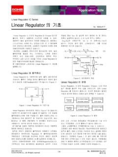
Linear Regulator IC Series Linear Regulator 기초
fscdn.rohm.comLinear Regulator 는 기본적으로 입력, 출력, GND 핀으로 구성되며, 출력이 가변일 경우는 출력전압의 귀환이 필요 하기 때문에 귀환(Feedback)핀이 추가됩니다. (Figure 1) IN OUT FB GND V IN V O Figure 1. Linear Regulator 의 기본구성 Linear Regulator 내부회로의 개요는 Figure 2 …

Op-Amp/Comparator Application Note - Rohm
fscdn.rohm.comop-amp. Generally, an op-amp is composed of three stages: the input stage, the gain stage, and the output stage. The input stage is configured with a differential amplification stage that amplifies the differential voltage between the two terminals. In addition, it does not amplify the common-mode signal component (a condition where no ...

Efficiency of Buck Converter
fscdn.rohm.comEfficiency of Buck Converter Switching regulators are known as being highly efficient power sources. To further improve their efficiency, it is helpful to understand the basic mechanism of power loss. This application note explains power loss factors and methods for calculating them.

Snubber Circuit for Buck Converter IC : Power Management
fscdn.rohm.comSnubber Circuit for Buck Converter IC AEK59-D1-0311-0 For example, when the input voltage VIN is 24 V and the switching frequency fSW is 1 MHz, 2 Ë Ì Ç » L680 pF H24 6 H1 MHz L0.39 W the generated consumption power of 0.39 W requires a 6432 size resistor (2512 in inches) with a rated power of 1 W.

ISO 26262: Functional Safety Standard for Modern Road …
fscdn.rohm.comIntrinsic safety is a method for ensuring safety by removing the causes of danger. Functional safety, on the other hand, is a method of reducing risks to an acceptable level to ensure safety ... verification, prototyping, and evaluation are clarified, with reviews performed at each stage. It is also necessary to manage the documents created at
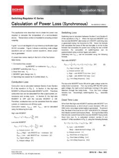
Calculation of Power Loss (Synchronous) : Power Management
fscdn.rohm.comCalculation of Power Loss (Synchronous) This application note describes how to obtain the power loss required to calculate the temperature of a semiconductor device. Temperature control is important to ensuring product reliability. Figure 1 is a circuit diagram of a synchronous rectification type DC/DC converter. Figure 2 shows a switching node ...
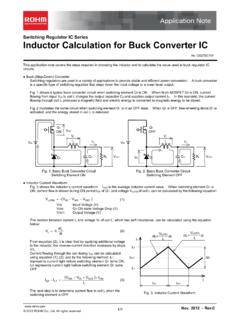
Inductor Calculation for Buck Converter IC
fscdn.rohm.comInductor Calculation of Buck Converter Current-difference between max. and min. (ILP-ILT) is as follows: IN SW D SW IN SW OUT D OUT LP LT V V V L f V V V V V I I (15) Equations (13) and (15) show that large inductance L and high switching frequency will reduce maximum current (ILP)and current difference between max. and min. (ILP-ILT).

Hysteresis Setting for Comparator - Rohm
fscdn.rohm.comprovided only to illustrate the standard usage and operations of the Products. The peripheral conditions must be taken into account when designing circuits for mass production. The technical information specified herein is intended only to show the typical functions of and examples of application circuits for the Products.
Related documents

富士パワーMOSFET - 富士電機
www.fujielectric.co.jp図1-4にこれまで開発した当社パワーMOSFET の系列を示します。 高耐圧Power MOSFET 低耐圧PowerMOSFET 1980 1990 1995 2000 2010 図1-4.富士パワーMOSFET 系列表 SIPMOS (F-0) F-Ⅰ F-Ⅱ FAP-Ⅱ FAP-ⅡA FAP-ⅡS series SuperFAP-G series SuperFAP-E3 series Super Junction MOSFET F-Ⅰ F-Ⅲ FAP-Ⅲ FAP-ⅢA

ON Semiconductor Is Now
www.onsemi.comapplication compare among regular, super junction MOSFET and even IGBT devices is feasible, while still using the same setup. It is important to mention that insulation barrier between primary and secondary side at MOSFET drivers level is provided …

Power MOSFET Selection Guide - NXP
www.nxp.comA MOSFET’s RDSon is given by the formula: RDSon = Rchannel + Rdrift + Rsubstrate + (Rpackage) Many manufacturers focus on reducing Rchannel to drive RDSon down. NXP’s Super-junction allows for an optimisation of all 3 components for reduction in RDSon, whilst also enhancing switching performance and Safe Operating Area. Maximising Switching ...

GAN POWER TRANSISTORS - Panasonic
eu.industrial.panasonic.comcon-based super-junction MOSFETs (see Figure 3). The Figure-of-Merit (RDS(on) ∙ QG) of a 600V/70nOhm GiT is value of modern silicon components. GATE DRIVING PRINCIPLE The GiT transistor is controlled as mix of a field effect transis-tor and (bi)polar transistor. As with FETs, a positive threshold

Super Junction MOSFET LLC コンバータの1次側スイッチン …
fscdn.rohm.comSuper Junction MOSFET シリーズ LLC コンバータの1次側スイッチング素子における PrestoMOSTM の有用性について LLC コンバータはインダクタL と容量C の共振を利用することによって、トランスの1 次側のスイッチング素子のターンON 時にゼロ電圧スイッチン

Power MOSFET Basics - Tayloredge
www.tayloredge.comtransistor (MOSFET) is based on the original field-effect transistor introduced in the 70s. Figure 1 shows the device schematic, transfer characteristics and device symbol for a MOSFET. The invention of the power MOSFET was partly driven by the limitations of bipolar power junction transistors (BJTs) which, until recently, was the device of ...

MOSFET Scaling - Department of Electrical and Computer ...
intra.ece.ucr.eduMOSFET Scaling Device scaling: Simplified design goals/guidelines for shrinking device ... • Doping gradient or junction abruptness limited by annealing process. ¾Polysilicon gate depletion ... SUPER-HALO Depth Doping Depth Doping Depth Doping 1E16 cm -3 5E16 cm -3 3E17 cm -3 1E18 cm -3 5E18 cm -3. 2/19/2003 19 Channel Profile Trends VV qN C ...

GaN Power HEMT Tutorial: GaN Basics
iganpower.comSuper Junction MOS SiC Cascode GaN PartID GPI65015TO xxxxxxxxx xxxxxxxxx xxxxxxxxx Rated Voltage 650V 700V 650V 600V Ron 92mΩ 125mΩ 100mΩ 150mΩ Qg 3.3nC 35nC 51nC 6nC Ron*Qg 304 4375 5100 900 Good: ØGaN is normally onby nature: easy to fabricate ØSi like gate control with higher Vth ØReverse conduction with LV MOS body-diode Bad: