Transcription of Snubber circuit design methods - Rohm
1 1/6 2017 ROHM Co., Ltd. No. 60AP001E 2020 ROHM Co., Ltd. No. 62AN037E Application Note SiC MOSFET Snubber circuit design methods SiC MOSFET is getting more popular in applications where fast and efficient switching is required, such as power supply applications. On the other hand, the fast switching capability causes high dv/dt and di/dt, which couple with stray inductance of package and surrounding circuit , resulting in large surge voltage and/or current between drain and source terminals of the MOSFET.
2 The surge voltage and current have to be controlled to not exceed the maximum rated voltage/current of the device. This application note illustrates a way to design Snubber circuit , which is one of the methods to suppress surges voltages and currents. Surge voltage occurring in Drain-Source When a MOSFET turns on, current stores energy in the stray inductance of the wire on the PCB layout. The stored energy resonates with the parasitic capacitance of the MOSFET, and that produces surge current.
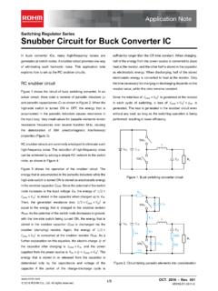
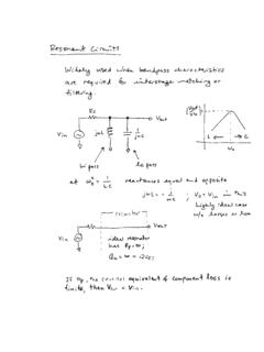
3 Figure 1 illustrates the path of the ringing current in a half bridge topology, which has high side switch (HS) and low side switch (LS). When LS turns on, current IMAIN flows from VSW through the stray inductance LMAIN. Figure 1 Current path when turn-off surge occurs When LS turns off, IMAIN flows through the loop form by LMAIN , CDCLINK and parasitic capacitance of HS and LS, as shown by dotted line. Where CDCLINK is bulk capacitor placed in parallel with input HVdc-PGND. During the turn off of LS, surge voltage occurs in drain-source of LS by resonant phenomenon between LMAIN and parasitic capacitance of the MOSFET COSS CDS+CDG.
4 The maximum voltage VDS_SURGE is as shown in (1). Where VHVDC is the applied voltage on HVdc terminal and ROFF is resistance when the MOSFET turns off. (*1). DS_SURGE= ( / )[tan 1( / )+ ]1+( )2 HVDC (1) where: A= HVDC +( / )2 (2 OFF MAIN HVDC)2 = 1 HVDC( / ) (2 OFF MAIN HVDC) =12 OFF OSS =1 MAIN OSS 1 ( MAIN/ OSS2 OFF)2 Figure 2 shows surge waveforms when ROHM s SiC MOSFET (SCT2080KE) turns off with 800V applied on HVdc. According to the waveform, VDS_SURGE reaches 961V and ringing frequency is about 33 MHz, which brings LMAIN of 110nH.
5 LS(LowSide)HS(HighSide)PGNDHVdcPGNDCDCLI NKLMAINVswIMAINIMAIN 2/6 2020 ROHM Co., Ltd. No. 62AN037E Application Note Snubber circuit design methods Figure 2. Turn-off waveform with surge Next step, a Snubber capacitor CSNB is introduced, as shown in Figure 3. This capacitor makes LMAIN neglectable. The waveform of the surge voltage when LS turns off is shown in Figure 4. Figure 3 C Snubber Surge voltage is reduced by more than 50V (reaching 901V) and ringing frequency increases to It is because CSNB is placed close to the switches and as a result, the stray inductances (LSNB) involved in the switching path is reduced.
6 In this case, LSNB is about 71nH according to the equation (1). It would be the best if stray inductance is minimized as much as possible. However it is not always realistic because it might make the heat dissipation condition worse. Instead, placing the Snubber capacitor as close as possible to the MOSFET minimize the stray inductance of the circuit . The Snubber capacitor also absorbs the energy stored in the minimized connection inductance and clamps surge voltage while the MOSFET turns off.
7 Figure 4. Reducing turn-off surge by C Snubber Variety and selection of Snubber There are two methods of Snubber circuits: passive Snubber , which consists of passive components such as resistor, inductor, capacitor and diodes; and active Snubber , which utilize semiconductor switch(*1 . In this application note, passive Snubber is chosen, due to its simplicity and cost effectiveness. Figure 5 shows different Snubber examples: (a) C Snubber , where the capacitor CSNB is connected in parallel to the MOSFET bridge; (b) RC Snubber where the resistor RSNB and capacitor CSNB are connected in parallel to each MOSFET; (c) Discharge RCD Snubber , where a diode is added to RC Snubber ; and (d) non-discharge RCD Snubber , where the discharging path is changed from the discharge RCD Snubber presented in (c).)
8 [A]VDS[V]Time [us]VDSIDVDS=800V, RG_EXT= [A]VDS[V]Time [us]without C Snubber1uF C SnubberVDSIDVDS=800V, RG_EXT= 3/6 2020 ROHM Co., Ltd. No. 62AN037E Application Note Snubber circuit design methods In principle, the Snubber has to be placed as close as possible to the MOSFET in order to maximize its effectiveness. (a) C Snubber : it has fewer components but has relatively longer wires. It is more suitable for 2in1 module rather than circuit with discrete components. (b) RC Snubber : it can be placed close to the MOSFET, however the energy stored in CSNB has to be dissipated by RSNB during every switching transient of the MOSFET.
9 If the switching frequency is high enough, RSNB would dissipate large amount of energy (several watts), which limits the size of CSNB. And, as results, the suppressing surge capability of the Snubber is reduced. (a) (b) (c) (d) Figure 5 Snubber circuits (a) C Snubber , (b) RC Snubber , (c) Discharge RCD Snubber , (d) Non-discharge RCD Snubber (c) Discharge RCD Snubber : RSNB dissipates energy as much as in (b) during turn ON, but CSNB surge absorption capability is more effective than (b) because surge current flows through the diode.
10 The recovery characteristic of the diode must be considered, high di/dt in the Snubber circuit can be occurred during the switching transient. Therefore, stray inductances should be minimized as much as possible to limit over voltages. It is also the same effect if RSNB is connected with CSNB in parallel . (d) Non-discharge RC Snubber : RSNB dissipates only the energy absorbed by CSNB produced during the overvoltage, it means the Snubber doesn t discharge all energy stored in CSNB at every switching transient.