Search results with tag "Gate driver"

MOSFET power losses and how they affect power-supply ...
www.ti.comGATE G TOT G SW= × ×Q V f ( ) (5) There are also general gate losses as shown in Figure 7. The MOSFET effect on the gate-driver IC, or a pulse-width modulation (PWM) controller with an integrated gate driver, add to the power-dissipation losses. As shown by Equation 6, gate-drive losses do not all occur on the MOSFET. P V Q 2 R R R R R R R R ...

High Voltage, Isolated Gate Driver with Internal Miller ...
www.analog.comcombination of pulse transformers and gate drivers. The . ADuM4121 /ADuM4121-1 operate with an input supply ranging from 2.5 V to 6.5 V, providing compatibility with lower voltage systems. In comparison to gate drivers that employ high voltage level translation methodologies, the ADuM4121/ ADuM4121-1 offer the benefit of true, galvanic isolation

Fundamentals of MOSFET and IGBT Gate Driver Circuits ...
www.ti.comprocedure for ground referenced and high side gate drive circuits, AC coupled and transformer isolated solutions are described in great details. A special section deals with the gate drive requirements of the MOSFETs in synchronous rectifier applications. For more information, see the Overview for MOSFET and IGBT Gate Drivers product page.
DRV8701 Brushed DC Motor Full-Bridge Gate Driver …
www.ti.com5.9V to 45 V DRV8701 H-Bridge Gate VREF Driver PH/EN or PWM Controller Gate drive sense output sense nSLEEP Shunt Amp Protection FETs nFAULT M LDO 3.3 & 4.8 V
DRV8302 Three Phase Gate Driver With Dual …
www.ti.comPWM DRV8302 8 to 60 V MCU N-Channel s Gate Drive Sense 3-Phase Brushless Gate Driver Buck Converter HW Control nFAULT nOCTW …

Fundamentals of MOSFET and IGBT Gate Driver Circuits ...
www.ti.comFundamentals of MOSFET and IGBT Gate Driver Circuits ... ... gate

Bootstrap Circuitry Selection for Half Bridge Configurations
www.ti.comto the gate driver supply pins. Figure 8 below shows a good layout example using UCC27710 with all bootstrap components located near the gate driver IC minimizing any effects of parasitic inductances and reducing the high peak currents path of the bootstrap circuit. It is also important to separate high voltage power and low voltage signal traces.

High Voltage, Isolated IGBT Gate Driver with …
www.analog.comHigh Voltage, Isolated IGBT Gate Driver with Isolated Flyback Controller Preliminary Technical Data ADuM4138 Rev. PrA Document Feedback Information furnished by Analog Devices is believed to be accurate and reliable.

Isolated Precision Half-Bridge Driver, 4 A Output Data ...
www.analog.comare 4 A isolated, half-bridge gate drivers that employ the Analog Devices, Inc., i. Coupler® technology to provide independent and isolated high-side and low-side outputs. The ADuM3223provides 3000 V rms isolation in the narrow body, 16-lead SOIC package, and the ADuM4223provides 5000 V rms isolation in the wide body, 16-lead SOIC package.
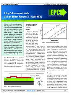
Using Enhancement Mode GaN-on-Silicon Power FETs …
epc-co.comUsing Enhancement Mode GaN-on-Silicon Power FETs (eGaN® FETs) Efficient Power Conversion Corporation’s (EPC) hyper-fast enhancement mode ... Below are the key characteristics of preferred gate drivers for EPC GaN transistors. For a controller to be functional with eGaN FETs, its driver would also need the following:
LTC4446 - High Voltage High Side / Low Side N …
www.analog.comLTC4446 1 4446f TYPICAL APPLICATION FEATURES APPLICATIONS DESCRIPTION High Voltage High Side/ Low Side N-Channel MOSFET Driver The LTC ®4446 is a high frequency high voltage gate driver that drives two N-channel MOSFETs in a …
BSS123 - N-Channel Logic Level Enhancement Mode Field ...
www.onsemi.comMOSFET gate drivers, and other switching applications. Features • 0.17 A, 100 V ♦ RDS(on) = 6 @ VGS = 10 V ♦ RDS(on) = 10 @ VGS = 4.5 V • High Density Cell Design for Extremely Low RDS(on) • Rugged and Reliable • Compact Industry Standard SOT−23 Surface Mount Package • This Device is Pb−Free and Halogen Free MARKING DIAGRAM

Motor Control Systems and Design - Analog Devices
www.analog.comtechnology, the isolated gate driver family offers the advantage of a maximum propagation delay of 50 ns, less than 5 ns channel-to-channel matching, a 50-year lifetime for 400 V rms working voltage, and galvanic isolation in a single package . Part Number
Similar queries
Gate, Driver, Gate driver, Providing, Galvanic, Gate drivers, DRV8302 Three Phase Gate Driver With Dual, DRV8302, Phase, MOSFET, Bootstrap Circuitry Selection for Half Bridge Configurations, Isolated, Isolated Flyback Controller Preliminary Technical Data ADuM4138, Analog Devices, Enhancement Mode GaN, Power, Enhancement mode, Channel MOSFET Driver, Channel