Inductive power transfer
Found 11 free book(s)
Understanding Shielded Cable - Mouser Electronics
www.mouser.comCables can be a main source of transfer for EMI, both as a source and receiver. As a source, the ... Notice that switching heavy loads, inductive heaters, large transformers can all present high levels of both conducted and radiated EMI. Placing signal cables next to power cables can also allow power-line noise to couple onto the
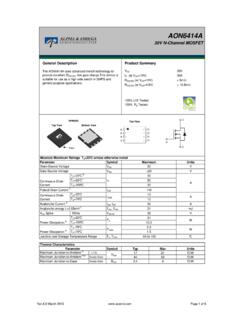
30V N-Channel MOSFET
www.aosmd.comReverse Transfer Capacitance VGS =0V, V DS =15V, ... The power dissipation P D is based on T J(MAX) =150 ... Unclamped Inductive Switching (UIS) Test Circuit & Waveforms Vds DSS 2 E = 1/2 LIAR AR Vgs Vdd Vgs Rg DUT-+ VDC Vgs Id Vgs I Ig Vgs-+ VDC DUT L Vgs Vds Isd Isd Diode Recovery Test Circuit & Waveforms Vds - Vds + IF AR dI/dt IRM rr Vdd ...
SERVICE CHECKER TYPE 3.1 INSTRUCTION MANUAL
my.daikin.eu5.4 Data transfer -----48 List of applicable models 50 Specifications-----50 ... radiation, inductive and/or capacitive coupling, for the treatment of material or inspection / ... Power switch When switching on, the red lamp is lit.

1.5KW to 6KW Any Power Combi Pure Sine Wave …
www.sigineer.comIt works bi-directionally: in one direction it converts DC power from the battery to AC power (Inverter Mode) and in the other direction it converts external AC power to DC power to charge the batteries (AC Mode). The same power components are used in both directions, resulting in high-energy transfer efficiency with fewer components.

UNIT 8 COORDINATE MEASURING Coordinate Measuring …
ignou.ac.inInductive and Optical Transmission Probes Inductive and optical transmission probes have been developed for automatic tool changing. Power is transmitted using inductive linking between modules fitted to the machine structure and attached to the probe. Figure 8.6 shows a schematic of the inductive transmission probe. The

TIP140 - Darlington Complementary Silicon Power Transistors
www.onsemi.comFigure 7. Unclamped Inductive Load L, UNCLAMPED INDUCTIVE LOAD (mH) 0.5 1.0 2.0 5.0 10 20 50 100 100 mJ INPUT MPS-U52 50 50 RBB1 1.5k RBB2 = 100 VBB2 = 0 VBB1 = 10 V TUT VCE MONITOR 100 mH VCC = 20 V IC MONITOR RS = 0.1 TEST CIRCUIT NOTE 1: Input pulse width is increased until ICM = 1.42 A. NOTE 2: For NPN test circuit reverse polarities. INPUT ...

Power MOSFET - Vishay Intertechnology
www.vishay.comFig. 12a - Unclamped Inductive Test Circuit Fig. 12b - Unclamped Inductive Waveforms Fig. 12c - Maximum Avalanche Energy vs. Drain Current Fig. 13a - Basic Gate Charge Waveform Fig. 13b - Gate Charge Test Circuit R G I AS tp 0.01 Ω D.U.T L V DS +-V DD 10 V Vary t p to obtain required I AS I AS V DS V DD V DS t p Q GS Q GD Q G V G Charge 10 V D ...

NCV8402 - Self-Protected Low Side Driver with Temperature ...
www.onsemi.comFigure 4. Single Pulse Maximum Inductive Switch−off Current vs. Time in Clamp TIME IN CLAMP (ms) I L(max) (A) TJstart = 25°C TJstart = 150°C 10 100 1000 110 Figure 5. Single Pulse Maximum Inductive Switching Energy vs. Time in Clamp TIME IN CLAMP (ms) E max (mJ) TJstart = 25°C TJstart = 150°C Figure 6. On−state Output Characteristics 0 ...

Cree C3M0025065D Silicon Carbide MOSFET
assets.wolfspeed.comInductive load Fig. 26 t r Rise Time 60 t d(off) Turn-Off Delay Time 27 t f Fall Time 12 R G(int) Internal Gate Resistance 1.3 Ω f = 1 MHz, V AC = 25 mV Q gs Gate to Source Charge 29 nC V DS = 400 V, V GS = -4 V/15 V I D = 33.5 A Per IEC60747-8-4 pg 21 Q gd Gate to Drain Charge 37 Fig. 12 Q g Total Gate Charge 108 Note (1): C
AC Electrical Circuit Analysis - MVCC
www2.mvcc.educompletes with chapters on AC power, resonance, and introductions to polyphase systems and magnetic circuits. Each chapter begins with a set of learning objectives and concludes with practice exercises that are generally divided into four major types: analysis, design, challenge and simulation. Many SPICE-based circuit simulators

AO3401 Rev6 Rohs-BUP007A
aosmd.comAO3401 Symbol Min Typ Max Units BV DSS-30 V VDS =-30V, V GS =0V -1 TJ=55°C -5 IGSS ±100 nA VGS(th) Gate Threshold Voltage -0.5 -0.9 -1.3 V ID(ON)-27 A 41 50 TJ=125°C 62 75 47 60 mΩ 60 85 mΩ gFS 17 S VSD-0.7 -1 V IS-2 A ISM-27 A Ciss 645 pF Coss 80 pF Crss 55 pF Rg 4 7.8 12 Ω Qg(10V) 14 nC Qg(4.5V) 7 nC Qgs 1.5 nC Q 2.5 nC Pulsed Body-Diode CurrentB Maximum Body-Diode …