Input Output And Storage
Found 9 free book(s)
Sia: Simple Decentralized Storage
sia.techoutput i in transaction t is de ned as: H(tjj\output"jji) where H is a cryptographic hashing function, and \output" is a string literal. The block reward and miner fees have special output IDs, given by: H(H(Block Header)jj\blockreward") Every input must come from a prior output, so an input is simply an output ID.
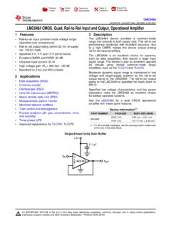
LMC6484 CMOS, Quad, Rail-to-Rail Input and Output ...
www.ti.comDifferential input voltage ±Supply Voltage Voltage at input/output pin (V−) −0.3 (V+) + 0.3 V Supply voltage (V+ −V−) 16 V Current at input pin(3) ±5 mA Current at output pin(4)(5) ±30 mA Current at power supply pin 40 mA TJ Junction temperature(6) 150 °C Tstg Storage temperature, Tstg −65 150 °C

Devices Input and Output UNIT 4 INPUT OUTPUT DEVICES
ignou.ac.in4.2 INPUT OUTPUT (I/O) DEVICES The computer will be of no use if it is not communicating with the external world. Thus, a computer must have a system to receive information from the outside world and must be able to communicate results to the external world. Thus, a computer consists of input/output devices. Input and output devices can also be ...
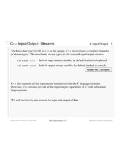
C++ Input/Output: Streams
courses.cs.vt.edu4. Input/Output Intro Programming in C++ C++ Input/Output: Streams The basic data type for I/O in C++ is the stream. C++ incorporates a complex hierarchy of stream types. The most basic stream types are the standard input/output streams: istream cin built-in input stream variable; by default hooked to keyboard ostream cout
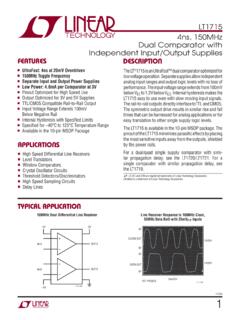
LT1715 Independent Input/Output Supplies FEATURES
www.analog.comIndependent Input/Output Supplies The LT ®1715 is an UltraFast™ dual comparator optimized for low voltage operation. Separate supplies allow independent analog input ranges and output logic levels with no loss of performance. The input voltage range extends from 100mV below V EE to 1.2V below V CC. Internal hysteresis makes the
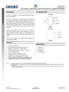
3 INPUT - Diodes Incorporated
www.diodes.comINPUT OUTPUT GND 10PF 22PF 3.3V V OUT =V REF * ( 1+R2/R1) + I ADJ * R2 3 1 2 2 1 3 Note 4: The AZ1117I is compatible with low ESR ceramic capacitor. The ESR of the output capacitors must be less than 20Ω. A minimum of 10µF output capacitor is required. Functional Block Diagram 2 Thermal Protection +-For Adjustable Output, disconnect A1 and A2 ...
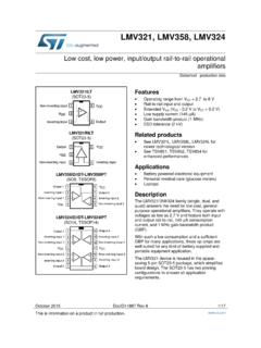
Datasheet - LMV321, LMV358, LMV324 - Low cost, low power ...
www.st.comOutput short-circuit duration See (7) 1. All voltage values, except differential voltage are with respect to network terminal. 2. The differential voltage is the non-inverting input terminal with respect to the inverting input terminal. If V. id > ±1 V, the maximum input current must not exceed ±1 mA. In this case (V. id
Understanding Digital Signal Processing
ptgmedia.pearsoncmg.com4.4 FFT Input/Output Data Index Bit Reversal 149 4.5 Radix-2 FFT Butterfly Structures 151 4.6 Alternate Single-Butterfly Structures 154 References 158 Chapter 4 Problems 160 5 FINITE IMPULSE RESPONSE FILTERS 169 5.1 An Introduction to Finite Impulse Response (FIR) Filters 170 5.2 Convolution in FIR Filters 175 5.3 Lowpass FIR Filter Design 186
Computers, part of your life Grade 10
www.studyopportunities.co.zai Computers, part of your life Grade 10 A textbook for Computer Applications Technology Sandra Jacobs Reinet Barnard Keith Gibson Ellen Labuschagne Pam Macmillan Pam Miller Chris Noomé