Silicon epitaxial
Found 12 free book(s)
1.EMITTER 2. BASE 3. COLLECT - atta.szlcsc.com
atta.szlcsc.comNPN silicon epitaxial planar transistor for switching and Amplifier applications As complementary type, the PNP transistor 2N3906 is Recommended This transistor is also available in the SOT-23 case with the type designation MMBT3904 MAXIMUM RATINGS (T A=25℃ unless otherwise noted) SymbolParameterValue Units V CBO Collector-Base Voltage 60 V V

SS8550 - PNP Epitaxial Silicon Transistor - ON Semiconductor
www.onsemi.comPNP Epitaxial Silicon Transistor SS8550 Features • 2 W Output Amplifier of Portable Radios in Class B Push−Pull Operation • Complementary to SS8050 • Collector Current: IC = 1.5 A • These Devices are Pb−Free, Halogen Free/BFR Free and are RoHS Compliant ABSOLUTE MAXIMUM RATINGS (TA = 25°C unless otherwise noted) Parameter Symbol ...
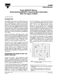
Power MOSFET Basics: Understanding MOSFET Characteristics ...
www.vishay.comepitaxial drain, into the substrate, and out of the wafer backside. The channel is formed under the polysilicon gate ... forms a grid surrounding islands of silicon. Each silicon island is the location of a double diffused channel region and its associated source diffusion.

2SC1815 2SC1815-O 2SC1815-Y 2SC1815-GR ... - mouser.com
www.mouser.comSILICON NPN TRANSISTORS DESCRIPTION: The CENTRAL SEMICONDUCTOR 2SC1815 Series are silicon NPN transistors, manufactured by the epitaxial planar process, designed for general purpose amplifier applications. MARKING: FULL PART NUMBER MAXIMUM RATINGS: (TA=25°C unless otherwise noted) SYMBOL UNITS Collector-Base Voltage VCBO 60 V
MEMS Fabrication I : Process Flows and Bulk Micromachining
www-bsac.eecs.berkeley.edu• Crystalline silicon is a hard and brittle material that deforms elastically until it reaches its yield strength, at which point it breaks. ... epitaxial layer Metal conductors Anodically bonded Pyrex substrate Etched cavity Backside port (111) R2 R1 R3 Deposit insulator Diffuse piezoresistors Deposit & …
A Manufacturing Cost and Supply Chain Analysis of ... - NREL
www.nrel.govSilicon carbide (SiC) is a WBG semiconductor material that is available for use in commercial power electronics systems. While the current SiC market is small, comprising less than 2% of ... A thin SiC epitaxial layer is then grown on top of this substrate to create an epi-wafer. The epi-wafer is processed to make SiC semiconductor devices ...

Axial Lead Rectifiers - ON Semiconductor
www.onsemi.commetal−to−silicon power diode. State−of−the−art geometry features chrome barrier metal, epitaxial construction with oxide passivation and metal overlap contact. Ideally suited for use as rectifiers in low−voltage, high−frequency inverters, free wheeling diodes, and polarity protection diodes. Features • Extremely Low VF

8-Ch/Dual 4-Ch High-Performance CMOS Analog Multiplexers
www.vishay.comDesigned in the 44 V silicon-gate CMOS process, the absolute maximum voltage rating is extended to 44 V. Additionally, single supply operation is also allowed. An epitaxial layer prevents latchup. For additional information please see Technical Article TA201. FEATURES • Low on-resistance - RDS(on): 100 • Low charge injection - Q: 20 pC

Silicon Wafer Processing - National Chiao Tung University
jupiter.math.nctu.edu.twGrowth of Epitaxial Silicon This step is done to provide a good clean surface for later processing. If a layer of Silicon is grown onto the top of the wafer using chemical methods then that layer is of a much better quality then the slightly damaged or unclean layer of silicon in the wafer. The epitaxial layer is where the actual processing will be
History of Semiconductors - Cornell University
djena.engineering.cornell.eduone. A transistor with epitaxial layer added was reported in 1960. In the same year Jean Hoerni proposed the pla-nar transistor (both base and emitter regions diffused). The oxide that served as a mask was not removed and acted as apassivatinglayer[15]. Further improvement of speed was proposed by Herbert Kroemer.
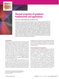
Thermal properties of graphene ... - Stanford University
poplab.stanford.edusuggested by experiments investigating epitaxial graphene on metals 25, 26 and recent theoretical work concerning graphene on insulators. 27 Figure 1. (a) Schematic of the atomic arrangement in graphene sheets. Dashed lines in the bottom sheet represent the outline of the unit cell. The areal density of carbon atoms in graphene

Atomic Layer Deposition - ALD Academy
www.aldacademy.comsilicon-based microelectronics industry began to in-crease.4,6 At that time, the method was also coined atom-ic layer deposition (ALD), a name which was more appro-priate considering the fact that the interest in amorphous films strongly increased. This increase was most promi-nent in highly-insulating oxide films to be used as low-