Transformer Design For Charging
Found 7 free book(s)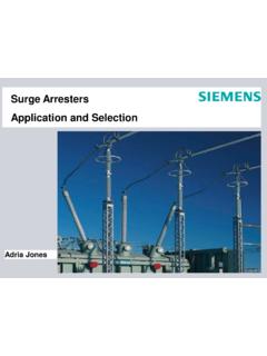
Surge Arresters Application and Selection
ewh.ieee.orgMounted in parallel to the transformer/equipment Handle over voltage surge, clamp it down ... Tube Design SR Hollow Core SR Tube Design SR WORKING 446,000 35,000 168,000 ... Line charging voltage 2) 2.6 2 2.6 Max rms L - G voltage i.e. MCOV 0.021 kJ/kV of MCOV

Medium Voltage Circuit Breaker Course Chapter 3.0 Student ...
www.nrc.gov• The charging spring normally charges automatically when the breaker is in ... Each breaker manufacturer operating mechanism design is different, but the electrical components required to operate the breaker all have similarities. Therefore, basic schematics for the control circuit for each manufacturer generally ... transformer performance ...

DC to DC Converters - Engineering
www.site.uottawa.caC charging i C = (i L – I out) ... •Design Criteria –Calculate the required inductor ... • Transformer volt-second balance is obtained over two switching periods • Effect of nonidealities? Boost Converter •As with the buck converter, the boost or step-

Inrush Current in DC-DC Converters - VPT, Inc.
www.vptpower.comThis peak current flows through the power transformer in the DC-DC converter to the output capacitor and into any load capacitance, charging them to their steady state value Figure 2. Typical inrush current waveform. Inrush Spike Current The first current peak is often referred to as the inrush spike. Its peak value and shape are highly

HANDBOOK of ELECTRIC VEHICLE CHARGING …
www.niti.gov.inAC and DC charging, power ratings, and charging standards. Covers the location and site planning aspects for EV charging, by framing the principles of location planning and demonstrating a methodology for spatial allocation of charging demand, and identifies enabling processes and policies to integrate public charging in urban planning.

MOSFETs Two-Switch Forward Converter: Operation, FOM, …
www.vishay.comThe second switching loss is that associated with charging and discharging of the MOSFET output capacitance Coss. In ATX power supplies, the popular two-switch forward converter follows the PFC converte r having an input voltag e ~400 V. As a result, the output switching loss can be a significant portion of the total losses.
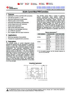
UCx84x Current-Mode PWM Controllers - Texas Instruments
www.ti.comcapacitance of the main switching FET used in the design. VCC 7 12 18 I Analog controller bias input that provides power to the device. Total VCC current is the sum of the quiescent VCC current and the average OUTPUT current. Knowing the switching frequency and the MOSFET gate charge, Qg, the average OUTPUT current can be calculated from: (2)