
AN032 PCB Technologies for LED Applications
The selection of appropriate materials for the circuit bo ard is therefore of utmost importance. FR4 printed circuit board (PCB) Classic composite PCB of glass fiber and epoxy resin, available in various compounds, versions (single-/ multilayer) and thickness (0.3 — 3.5 mm). Table 1: FR4 PCB versions Designation Material Note
Download AN032 PCB Technologies for LED Applications

Information
Domain:
Source:
Link to this page:
Documents from same domain

AN021 Further details on lead-free reflow soldering of LEDs
dammedia.osram.infoFurther details on lead-free reflow soldering of LEDs Abstract The interaction between RoHS-compliant SMD components and lead-free processing can ... Due to the conditional reduction of the process window for the lead-free solder materials, increased attention must be paid to …

AN048 The Basic Principles of Electrical Overstress (EOS)
dammedia.osram.infoMany OSRAM Opto Semicond uctors LEDs have ESD pr otection devices that are meant to protect the LED from ESD even ts. OSRAM Opto Semiconductors latest products are protected up to 8 kV HBM (human body mode l) or up to 15 kV acc. to IEC 61000-4-2 (air discharge). Features SYNIOS® P 2720: • Package: SMD epoxy package • Technology: UX:3

AN122 Chemical compatibility of LEDs - dammedia.osram.info
dammedia.osram.infochemical compatibility based on certain material components but not on commercial products, as the chemical components within each commercial product are subject to change without notice. Unfortunately, it would not be possible to include all chemicals, given that LEDs are subjected to very diverse

AN109 Dry pack information - dammedia.osram.info
dammedia.osram.infoThe card may be reused as long all the sensors elements are blue. Dry pack labels The following two labels are applied to the outside of the dry pack bag: A standard Barcode-Product-Label (BPL), identifies the contents by: producer (OSRAM Opto Semiconductors), country of origin, product designation, lot number, date code, material number and ...

www.osram.de/ledcheck
dammedia.osram.infoNIGHT BREAKER ® LED Produktbezeichnung Typ V W K EAN10 64210DWNB H7-LED 12 14 6000 4062172155045 H7-LED Fahrzeugliste – PKW …

AN006 Reliability and lifetime of LEDs
dammedia.osram.infoof customer expectations over the expected lifetime. In other words, the LED does not fail during its lifetime under the given environmental and functional conditions. The reliability of the products is thus based on the chain of the materials, the manufacturing process and the function of the component (Figure 1).
Related documents

PCI Express* Board Design Guidelines
www.linelayout.comlayouts onto Printed Circuit Boards (PCB) ranging from 4-layer desktop baseboard designs to 10-layer or more server baseboard designs. Guidelines and constraints in this document are intended for use on both baseboard and add-in card PCB designs. This includes interconnects between PCI

0.3mm Pitch 1.1mm Height Top and Bottom Contact Back-Flip ...
www.farnell.com0.2mm thick standard Flexible Printed Circuit (FPC) can be used. This is the only ultra-low profi le ZIF connector using standard FPC. 6. Conductive traces on the PCB can run under the connector No exposed contacts on the bottom of the connector. 7. Board placement with automatic equipment Flat upper surface and tape and reel packaging

IIT Kanpur PCB Design Guide Sheet
iitk.ac.inThe conductive circuit is generally copper, although aluminum, nickel, chrome, and other metals are sometimes used. There are three basic varieties of printed circuit boards: single‐sided, double‐sided, and multi‐ layered. 1. Single sided PCB: conductors on only one surface of a dielectric base. 2.
How to Build a Printed Circuit Board - 4pcb.com
www.4pcb.comHow to Build a Printed Circuit Board. Advanced Circuits Inc 2004 2 This presentation is a work in progress. As methods and processes change it will be updated accordingly. It is intended only as an introduction to the production processes used in building a circuit board and as a training aid for employees, customers and friends of Advanced ...

AN136 - PCB Layout Considerations for Non-Isolated ...
www.analog.comto the printed circuit board (PCB) layout, identifying the cause can be difficult. This is why proper PCB layout at the early stage of a switching supply design is very critical. Its importance cannot be overstated. The power supply designer is the person who best under-stands the technical details and functional requirements of
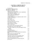
CHAPTER 12: PRINTED CIRCUIT BOARD (PCB) DESIGN ISSUES
www.analog.comCHAPTER 12: PRINTED CIRCUIT BOARD (PCB) DESIGN ISSUES Introduction Printed circuit boards (PCBs) are by far the most common method of assembling modern electronic circuits. Comprised of a sandwich of one or more insulating layers and one or more copper layers which contain the signal traces and the powers and grounds, the

PCB Rework and Repair Guide - Intertronics
www.intertronics.co.ukThe repair specialists at Circuit Technology Center, Inc. have used this guidebook to repair thousands of PC boards. Circuit Technology Center, Inc. i s the world's leading specialist in PC board repair and modification and the procedures described herein are the same procedures they use to repair and modify PC boards.