
Analog Discovery ™ Technical Reference Manual
differential, 14 bit, 100Msample/sec, 5MHz bandwidth) • Two-channel arbitrary function generator (22Ω, ±5V, 14 bit, 100Msample/sec, 5MHz bandwidth) • Stereo audio amplifier to drive external headphones or speakers with replicated AWG signals • 16-channel digital logic analyzer (3.3V CMOS, 100Msample/sec)*
Download Analog Discovery ™ Technical Reference Manual

Information
Domain:
Source:
Link to this page:
Documents from same domain
Nexys4 DDR™ FPGA Board Reference Manual - Digilentinc
digilent.comType A USB Host Connector (J5) Serial Prog. Port 2 6-pin JTAG Header (J10) Prog Micro SD Connector (J1) Media Select (JP2) User I/O M2 Mode (JP 1) Programming Mode JP2 JP1 NA SPI Flash NA JTAG USB MicroSD Figure 3. Nexys4 DDR configuration options. Figure 3 shows the different options available for configuring the FPGA. An on-board “mode ...
Basys 3™ FPGA Board Reference Manual - Digilent Reference
digilent.comPIC24 Type A USB Host Connector (J2) Serial Prog. Port 2 6-pin JTAG Header (J5) Prog M2 Mode (JP1) Programming Mode JP1 SPI Flash JTAG USB Figure 3. Basys 3 configuration options. The FPGA configuration data is stored in files called bitstreams that have the .bit file extension. The Vivado

ZedBoard HW Users Guide - Digilent Reference
digilent.comAug 01, 2012 · DDR3 on the PS was routed with 40 ohm trace impedance for single-ended signals, and DCI resistors (VRP/VRN) as well as differential clocks set to 80 ohms. Each DDR3 chip needs its own 240-ohm pull-down on ZQ. DDR-VDDQ is set to 1.5V to support the DDR3 devices selected. DDR-VTT is the termination voltage which is ½ DDR-VDDQ.

Nexys A7 FPGA Board Reference Manual - Digilentinc
digilent.comThe major improvement from the Nexys 4 to the Nexys 4 DDR is the replacement of the 16 MiB Cellular RAM with a 128 MiB DDR2 SDRAM memory. Furthermore, to accommodate the new memory, the pin-out of the FPGA banks changed as well. The audio output (AUD_PWM) needs to be driven open-drain as opposed to push-pull on the Nexys 4. 1 Functional Description

Zybo Z7 Board Reference Manual - Digilentinc
digilent.com• High-bandwidth peripheral controllers: 1G Ethernet, USB 2.0, SDIO • Low-bandwidth peripheral controllers: SPI, UART, CAN, I2C • Programmable from JTAG, Quad-SPI flash, and microSD card • Programmable logic equivalent to Artix-7 FPGA

Arty™ FPGA Board Reference Manual - Digilent Reference
digilent.comport (J10) or it can be derived from a 7 to 15 Volt D power supply that [s connected to Power Jack (J12) or Pin 8 of Header J7. Header J13, located between the power jack and the Ethernet connector, is used to determine which source is used. A power-good LED (LD11), driven by the power good _ (PWRGD) output of the ADP5052 regulator, indicates that

ZYBO - Digilentinc
digilent.comMay 31, 2017 · zybo z7 board digilen t inc. a vailable on z20 v er sion only pibtn401 pibtn402 pibtn403 cobtn4 pibtn404 pibtn501 pibtn502 pibtn503 cobtn5 pibtn504 pid101 pid102 pid103 pid104 pid105 cod1 pid201 pid202 pid203 pid204 pid205 cod2 pid301 pid302 pid303 pid304 pid305 cod3 pid401 pid402 pid403 pid404 pid405 cod4 ...

Analog Discovery 2™ Reference Manual
digilent.comStereo audio amplifier to drive external headphones or speakers with replicated AWG signals 16-channel pattern generator (3.3V CMOS, 100Msample/sec)i ii 16-channel virtual digital I/O including buttons, switches, and LEDs – perfect for logic training applicationsiii iv 16-channel digital logic analyzer (3.3V CMOS,
Digilent Pmod Interface Specification
digilent.comhost controller boards. There are six-pin and twelve-pin versions of the interface defined. The six-pin ... Microcontroller system boards are generally provided with dedicated I 2C connectors and provide pull-up resistors that are jumper selectable to be in or out of circuit. FPGA based system boards generally

Introduction to Digital Design Using Digilent FPGA Boards
digilent.comExample 9 – 7-Segment Decoder 48 Example 10 – 7-Segment Displays: x7seg and x7segb 54 Example 11 – 2's Complement 4-Bit Saturator 64 Example 12 – Full Adder 70 ... digital circuit and implement it by connecting the internal gates in a particular way. This
Related documents

Automatic Gain Control (AGC) in Receivers
www.qsl.netwill slow any undesired interactions from taking place between all of the gain-controlled stages. Transistor amplifiers require special circuits or devices for amplifier stage gain control. One circuit arrangement for this application uses one gate of a dual-gate FET as the gain control device while the signal is applied to the second gate.

B.Tech. 3rd Year V Semester ECE Scheme
aktu.ac.inB.Tech. 3rd Year V Semester ECE Syllabus KEC-501 Integrated Circuits 3L:1T:0P 4 Credits Unit Topics Lectures I The 741 IC Op-Amp: General operational amplifier stages (bias circuit, the input stage, the second stage, the output stage, short circuit protection circuitry), device

G631 Product Catalog - Moog Inc.
www.moog.comof a polarized electrical torque motor and two stages . of hydraulic power amplification. The motor armature ... The flapper of the first stage hydraulic amplifier is rigidly . attached to the armature. The flapper extends through the ... can be made for series, parallel, or differential operation. G631/631 Series Servo Valves can be supplied ...
CMOS Comparator Design
www.eecis.udel.eduA fully-differential gain-stage Avoid or use simple CMFB Pre-amp gain reduces input referred offset due to the latch Autozeroing techniques for offset storage and reduction Pre-amp open-loop gain vs tracking bandwidth trade-off Multiple stages of pre-amp limit bandwidth • Optimum value of stages 2-4 §· 00 §·

Audio Power Amplifier - de Smith
www.desmith.net4. The small signal stages 75 5. The output stage I 109 6. The output stage II 166 7. Compensation, slew-rate, and stability 186 8. Power supplies and PSRR 239 9. Class-A power amplifiers 259 10. Class-G power amplifiers 294 11. Class-D amplifiers 319 12. FET output stages 328 13. Thermal compensation and thermal dynamics 339 14. The design ...
Fast, Voltage-Out, DC to 440 MHz, 95 dB Logarithmic ...
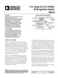
www.analog.comFully differential dc-coupled signal path . 100 ns power-up time, 1 mA sleep current . ... AMPLIFIER STAGES ... 01084-001 Figure 1. GENERAL DESCRIPTION . The AD8310 is a complete, dc to 440 MHz demodulating logarithmic amplifier (log amp) with a very fast voltage mode output, capable of driving up to 25 mA into a grounded load in
Fundamental Signal Conditioning - mccdaq.com
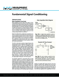
www.mccdaq.comfollower and the difference amplifier. Inverting Amplifier Stages The inverter stage is the most basic operational amplifier configuration. It simply accepts an input signal referenced to common, amplifies it, and inverts the polarity at the output terminals. The open-loop gain of a typical operational amplifier is in the hundreds of thousands.