
Basic OpAmp Design and Compensation
this will have less voltage drop. (but it is not used when there is only capacitive load). Fourth, noise is a concern. Typically, pMOS helps reduce the noise. In summary, when using a two-stage OpAmp, the pMOS input stage is preferred to optimize w ta and minimize noise.
Download Basic OpAmp Design and Compensation

Information
Domain:
Source:
Link to this page:
Documents from same domain

What is Restorative Justice -- revised2
www.d.umn.edurestorative justice briefing paper - 2 centre for justice & reconciliation at prison fellowship international may 2005 po box 17434, washington, dc 20041♦phone 703.481.0000♦fax 703.481.0003♦email dvanness@pfi.

Motivation In Sport - University of Minnesota Duluth
www.d.umn.eduWhat do coaches want from the study of motivation? Higher task achievement from their athletes High task persistency from their athletes Higher effort from their athletes
ECE 1315 Digital Logic Design Laboratory Manual
www.d.umn.eduECE 1315 Digital Logic Design Laboratory Manual ... equipment that you will use in the lab to build and test ... display digital inputs and outputs from your ...

ANTICOAGULANT, THROMBOLYTIC, and ANTI …
www.d.umn.eduMed 6541 Hematopoiesis and Host Defences Spring 2006 Dr. Janet Fitzakerley 307 Med jfitzake@d.umn.edu Anticoagulants www.d.umn.edu/~jfitzake Page 1 of 21
Experiential Learning Theory - University of …
www.d.umn.eduExperiential Learning Theory: Previous Research and New Directions David A. Kolb Richard E. Boyatzis Charalampos Mainemelis Department of Organizational Behavior

Analog Integrated Circuit Design 2nd Edition
www.d.umn.eduto the design of a comparator. Random circuit noise can cause the output to change from one logic level to the other, even when the comparator input is held constant. Hence, in order to measure the input offset

Analog Integrated Circuit Design
www.d.umn.edu• Good analog circuit designers are scarce (very well compensated, gain lots of respect, regarded as “artists” because of the “creative” circuit design they do…
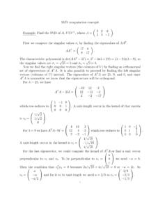
SVD computation example A U V T A 3 2 2 AA
www.d.umn.eduSVD computation example Example: Find the SVD of A, UΣVT, where A = 3 2 2 2 3 −2 . First we compute the singular values σ i by finding the eigenvalues of AAT. AAT = …
PER UNIT IDENTITIES - University of Minnesota Duluth
www.d.umn.eduECE 4501 POWER SYSTEMS UMD PER UNIT IDENTITIES DISCUSSION: Per Unit (pu) systems are used by engineers to quantify equipment parameters in terms of their Nameplate
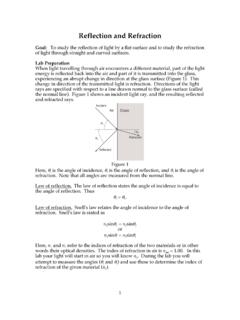
Lab 8 Reflection and Refraction
www.d.umn.edu1" " Reflection and Refraction Goal: To study the reflection of light by a flat surface and to study the refraction of light through straight and curved surfaces. Lab Preparation When light travelling through air encounters a different material, part of the light
Related documents

THE SIMPLE HIGH-VOLTAGE REGULATOR
www.next-tube.comFor solid-state devices with rather low voltage the realization of a high-quality source does not represent the special problems. With high-voltage power supplies for tube amplifiers the states of affairs are much worse. A certain vacuum here was formed. First, there are no suitable microcircuits directly designed for work with high voltage.

931 Signal Conditioners - Rockwell Automation
literature.rockwellautomation.com• Powered by 24V DC, compatible for power bus DIN system 931N-A222: Analog Signal Splitter • Provides two isolated output signals from one input signal, which can be used for local HMI or other use • Four-way galvanic isolation between power supply, input, 2 outputs • Powered by 24V DC, compatible for power bus DIN system

A Simple Regen Radio for Beginners - ARRL - Home
www.arrl.orgproject box using small screws. Mount the headphone jack on the box rear, close to the PC board and the LM386. Attach the RadioShack 39-inch whip antenna to one of the back corners of the box using a small screw and nut. If you use the RadioShack jack specified for J1 (RS 274-276), connect together pins 2 and 5 and attach that common lead to C8.

Power Station2 Manual - Fryette Amplification
fryette.combefore using the amplifier at high power levels with the power station connected. output tubes can easily fail when stressed. catastrophic tube failure can also damage other components such as the output transformer. x the power station is not intended for use with solid state amplifiers that use current feedback and an ungrounded output.

Photodiode/Phototransistor Application Circuit
physlab.orgrent amplification so that the signal is greatly amplified. AMPLIFIER CIRCUIT USING OPERATIONAL AMPLIFIER Figure 13 shows a current-voltage conversion circuit using an operational amplifier. Its output voltage (VOUT) is expressed as VOUT = IC × R1. The current-voltage conversion circuit for the pho-totransistor is basically identical to that ...
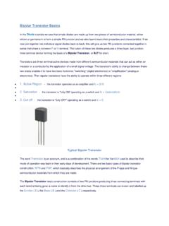
Bipolar Transistor BJT - University of Pittsburgh
sites.pitt.eduThis type of amplifier configuration is a non-inverting voltage amplifier circuit, in that the signal voltages . Vin. and . Vout. are in-phase. This type of transistor arrangement is not very common due to its unusually high voltage gain characteristics. Its output characteristics represent that of a forward biased diode while the input ...

a Low Noise, Precision, High Speed Operational Amplifier ...
www.analog.comDec 20, 1980 · 2.7 Hz, and the high gain of 1.8 million, allow accurate high-gain amplification of low-level signals. The low input bias current of 10 nA and offset current of 7 nA are achieved by using a bias-current cancellation circuit. Over the military temperature range this typically holds I B and I OS to 20 nA and 15 nA respectively. PIN CONNECTIONS

Operational amplifier, Comparator (Tutorial)
www.mouser.comresistor, and AV is the amplification factor of the op-amp. The relation between the input and output voltages is described in the equation (1.1.1). (1.1.1) As shown in Figure 1.1.2 and the equation (1.1.1), the signal voltage VS is divided into resistance voltages by the signal source resistor RS and the input resistor Ri of the op-amp. As

Demystifying Type II and Type III Compensators Using Op ...
www.ti.comSLVA662 4 Demystifying Type II and Type III Compensators Using Op-Amp and OTA for DC/DC Covverters 2 Type II Compensator Using Op-Amp Offering an origin pole, one zero, and one high-frequency pole, the Type II compensator provides a phase boost up to 90 degrees.

System-Leve ESD Protection Guide (Rev. C)
www.ti.coma ±3 .6-V working voltage making it a suitable solution for antenna applications . ESD Solutions for Antenna Applications WiFi Transceiver Power Amplifier Filtering Network Device Working Voltage (V) IEC 61000-4-2 ESD Rating (kV) (Contact/Air Gap) Capacitance (pF) Channels Package Size (mm) Package TPD1E0B04DPY ±3.6 8/9 0.13 1 1.0 x 0.6 0402