
Breakdown in Solid Dielectrics - BU
When solid dielectrics are subjected to high electric fields, failure occurs due to electrostatic compressive forces which can exceed the mechanical compressive strength. If the thickness of the specimen is d0 and is compressed to thickness d under an applied voltage V, then the electrically developed compressive stress is in equilibrium.
Download Breakdown in Solid Dielectrics - BU

Information
Domain:
Source:
Link to this page:
Documents from same domain

MECHANICAL PROPERTIES OF ENGINEERING MATERIALS
www.bu.edu.egMaterials scientists learn about these mechanical properties by testing materials. Results from the tests depend on the size and shape of material to be tested (specimen), how it is held, and the way of performing the test.

1. AACE Practice No. - Bu
www.bu.edu.egThe World Bank and the International Finance Corporation (IFC), “Doing Business 2010 Egypt, Arab Republic” , The International Bank for Reconstruction and Development / The World Bank, 2009.

Introduction to Three-phase Circuits
www.bu.edu.eg• Three phase is the most economical polyphase system. AC Generation • Three things must be present in order to produce electrical current: a) Magnetic field b) Conductor c) Relative motion • Conductor cuts lines of magnetic flux, a voltage is induced in the conductor

General Pathology Notes - BU
www.bu.edu.egCause of injury – ischaemic, physical, chemical, infectious, immunological Time course – rapid and acute, or slow and chronic (depends on the pathogenic mechanism, persistence of the injurous agent and presence of certain cell types) Initial reactions – localized, non-specific systemic manifestations (e.g. pyrexia)
7 Measurement of High Voltages and Currents
www.bu.edu.egresistors located in an airtight transformer oil filled P.V.C. tube, for 100 kV operation had very good temperature stability. The limitations in the series resistance design are: (O power dissipation and source loading, (ii) temperature effects and long time stability, (Ui) voltage dependence of resistive elements, and
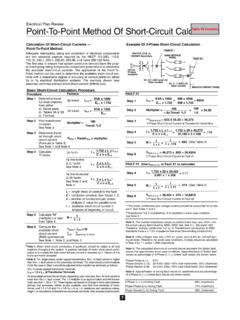
Electrical Plan Review Point-To-Point Method Of Short ...
www.bu.edu.eg440 59 98 148 197 295 394 656 984 1312 1968 2624 460 56 94 141 188 282 377 628 941 1255 1883 2510 480 54 90 135 180 271 361 601 902 1203 1804 2406 600 43 72 108 144 217 289 481 722 962 1443 1925 Electrical Plan Review Point-To-Point Method Of Short-Circuit Calculation Ampacity Busway Plug-In Feeder High Impedance Copper Aluminum Copper Aluminum ...
Chapter 2 Field crop classification
www.bu.edu.egThis family includes about three fourths of the cultivated forage crops and all the cereals. They have the following characters: - They are winter annuals or perennials. - They are almost herbaceous plants. - Stems are usually hollow, cylindrical and made up of nodes and internodes. - Leaves are alternative with parallel veins.
MECHANICAL PROPERTIES OF ENGINEERING MATERIALS
www.bu.edu.egthe mechanical properties of a material. The test is performed using a loading apparatus such as the Tinius Olsen machine. The capacity of this machine is 10,000 pounds (tension and compression). The specimen of a given material (i.e. steel, aluminum, cast iron) takes a cylindrical shape that is 2.0 in. long and 0.5 in.

Chapter 5 BJT Biasing Circuits
www.bu.edu.eg1. Determine the Q-point and construct dc load line for this transistor. Figure 5.26 For problem 1. [7] 2. Assume DC = 100 and I E I C. (a) Find V E, V C (b) Determine Q-point of this transistor (c) Construct DC load line and plot Q-point (d) Calculate IC if R B is changed from 10 k to be 1 k Figure 5.27 For problem 2.

Lecture #4 BJT AC Analysis
www.bu.edu.eg• The dc analysis of npn and pnp configurations is quite different in the sense that the currents will have opposite directions and the voltages opposite polarities. • However, for an ac analysis where the signal will progress between positive and negative values, the ac equivalent circuit will be the same. npn versus pnp J-601-4 l-a
Related documents
BSIM4.3.0 MOSFET Model - CMOSedu.com
cmosedu.comdifferent from 3.9 (SiO 2) as an alternative approach to modeling high-k dielectrics. Figure 1-1 illustrates the algorithm and options for specifying the gate dielectric thickness and calculation of the gate dielectric capacitance for BSIM4 model evaluation. Figure 1-1. Algorithm for BSIM4 gate dielectric model.
The Relationship Between Loss, Conductivity, and ...
pleclair.ua.eduNov 13, 2001 · In dielectrics, this term usually dominates the first term. In metals, the real part of the permittivity is usually equal to the permittivity of free space, and the imaginary part is usually zero. Semiconductors maintain a relative balance between the two terms.

INTERNATIONAL
irds.ieee.orgprocess changes such as high- κ gate dielectrics and strain enhancement, and in the near future, new structures such as gate-all-around (GAA); alternate high-mobility channel materials, and new 3D integration schemes allowing heterogeneous stacking/integration. These innovations be introduced at a rapid pace, and hence understanding, modeling ...

Film Capacitors - Vishay Intertechnology
www.vishay.com• Dielectrics according to IEC 60062: KT = Polyethylene terephthalate (PET) KP = Polypropylene (PP) KI = Polyphenylene sulfide (PPS) KN = Polyethylene naphtalate (PEN) • Polyethylene terephthalate (PETP) and polyethylene naphtalate (PEN) films are generally used in general purpose capacitors for