DRAM Technology - Smithsonian Institution
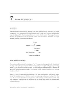
OVERVIEW DRAM (Dynamic Random Access Memory) is the main memory used for all desktop and larger computers. Each elementary DRAM cell is made up of a single MOS transistor and a storage capacitor (Figure 7-1). ... Design improvements allow for the decrease in …
Download DRAM Technology - Smithsonian Institution

Information
Domain:
Source:
Link to this page:
Documents from same domain

Profitability in the Semiconductor Industry
smithsonianchips.si.eduProfitability in the Semiconductor Industry 1-2 INTEGRATED CIRCUITENGINEERING CORPORATION From year to year, the health of the semicon-ductor industry as a whole is indicated by its

Section 4 Worldwide ASIC Market - Smithsonian …
smithsonianchips.si.eduthe total logic market mirrored the MOS logic segment. PROS AND CONS OF ASICs ... Worldwide ASIC Market 4-4 INTEGRATED CIRCUIT ENGINEERING CORPORATION

Yield and Yield Management - Smithsonian Institution
smithsonianchips.si.edusemiconductor industry. Line yield refers to the number of good wafers produced with-out being scrapped, and in general, measures the effectiveness of material handling, process control, and labor. Die yield refers to the number of good dice that pass wafer probe testing from wafers that reach that part of the process. It is intended to prevent

Changing Wafer Size and the Move to 300mm
smithsonianchips.si.eduwafer. Unfortunately, due to equipment pro-ductivity and price increases for larger wafer processing tools, the cost savings resulting from wafer size transitions may not scale with these die per wafer calculations. For instance, 200mm wafers offer nearly twice the area of 150mm wafers (1.78X), but many early adopters of 200mm technology argue
Related documents

DRAM Design Overview - Stanford University
www.graphics.stanford.eduDRAM Design Overview Junji Ogawa ASSP/ASIC Standard Operating Frequency Customizability WRAM VRAM DRAM/Logi c SLDRAM CDRAM EDRAM EDO MDRAM Function rich DRAM 100MHz 200MHz 500MHz DDR 1GHz 2GHz High-speed DRAM Target SDRAM RAMBUS DRAM Operating Frequency v.s. Customizability Feb. 11th. 1998 DRAM Design Overview Junji Ogawa

NAND vs. NOR Flash Memory Technology Overview
aturing.umcs.maine.eduApr 25, 2006 · DRAM in which the program code can be shadowed and run. In either case, the different types of memory are frequently stacked in Multi-Chip Packages (MCP) to create a single component. This overview will briefly discuss the history of …

SEMICONDUCTOR MEMORIES - University of California, …
bwrcs.eecs.berkeley.eduThe read-out of the 1T DRAM cell is destructive; read and refresh operations are necessary for correct operation. Unlike 3T cell, 1T cell requires presence of an extra capacitance that must be explicitly included in the design. When writing a “1” into a DRAM cell, a threshold voltage is lost.

Memory Basics - Michigan State University
www.egr.msu.edu– Dynamic: will lose data unless refreshed periodically (DRAM) ECE 331, Prof. A. Mason Memory Overview.2 SRAM/DRAM Basics •SRAM: Static Random Access Memory – Static: holds data as long as power is applied –Volatile: can not hold data if power is removed – 3 Operation States: hold, write, read – Basic 6T (6 transistor) SRAM Cell

Understanding DRAM Operation - Computer Architecture …
compas.cs.stonybrook.eduUnderstanding DRAM Operation 12/96 Page 1 Overview Dynamic Random Access Memory (DRAM) devices are used in a wide range of electronics applications. Although they are produced in many sizes and sold in a variety of packages, their overall operation is essentially the same. DRAMs are designed for the sole purpose of storing data.

TN-41-13: DDR3 Point-to-Point Design ... - Micron Technology
www.micron.comright memory design methodology can be critical to a project’s success. While DDR3 SDRAM was targeted for use on modules, it can easily be adapted for point-to-point ap-plications. DDR3 is an evolutionary transition from DDR2. DDR3 point-to-point systems are simi-lar to DDR2 point-to-point systems; both require similar design principles. But ...

Chapter 1: HIR Overview and Executive Summary
eps.ieee.orginnovation in design and process technologies continue the drive to advanced nodes, Moore’s-Law economics and performance are evidently plateauing. Shown below are two graphs presented by John Hennessy at the ERI Conference in July 2018 [5]. The graph to the left shows forty years of DRAM capacity and the slowing down of

TN-ED-04: GDDR6 Design Guide - Micron Technology
www.micron.comsignal is such that it is always sourced from DRAM to controller, for both reads and writes. Due to this, extra care is recommended during PCB design and analysis ensuring the EDC net is evaluated for both near-end and far-end crosstalk. TN-ED-04: GDDR6 Design Guide GDDR6 Overview CCM005-524338224-10517 tn_ed_04_gddr6_design_guide.pdf - Rev. B ...