
ELECTRONICS AND COMMUNICATION ENGINEERING …
UNIT 6: CMOS VLSI SYSTEMS MOSFET's as switches, Basic logic gates in CMOS, CMOS layers, CMOS inverter, Dynamic CMOS, Floor planning and Routing, Low power design, Reliability and testing of VLSI circuits, CMOS clocking an d testing; Structural Gate Level Modeling; Switch Level Modeling; Behavioral and RTL Modeling — Multiplier, encoders,
Download ELECTRONICS AND COMMUNICATION ENGINEERING …

Information
Domain:
Source:
Link to this page:
Documents from same domain
Syllabus : English - Teachers Recruitment Board
trb.tn.nic.inFor the post of Written Recruitment Test for the post of Postgraduate Assistants in Tamil Nadu Higher Secondary Educational Service. Syllabus: English (Subject Code: P02) Unit-I – MODERN LITERATURE (1400-1600)

TET Paper 1 English - Teachers Recruitment Board
trb.tn.nic.in(iii) Language II English (Classes i to V) Class I 1. Listening Competency Content Mode of Transaction Evaluation · Listening to jingles / Nursery rhymes
download Syllabus - Tn - Teachers Recruitment Board
trb.tn.nic.inTAMIL NADU GOVERNMENT GAZETTE EXTRAORDINARY UNIT -3 METHODS OF PHYSICAL EDUCATION. Principles of Class Management — Formation — Types of commands — Methods, Ora', Demonstration, limitation
MECHANICAL ENGINEERING UNIT 1: …
trb.tn.nic.inMECHANICAL ENGINEERING UNIT 1: ENGINEERING MATHEMATICS Linear Algebra: Matrix algebra, Systems of linear equations, Eigen values and eigen vectors. Calculus: Functions of single variable, Limit, continuity and differentiability, Mean
TET Paper 2 Child Development & Pedagogy
trb.tn.nic.inTeachers Eligibility Test - Paper 2 i. Child Development and Pedagogy (Relevant to Age Group 11 – 14) UNIT I: Nature of Educational Psychology
TET Paper 1 Child Development and Pedagogy - t n
trb.tn.nic.inTeachers Eligibility Test - Paper 1 (i) Child Development and Pedagogy (Relevant to Age Group 6 - 11) Part (A): Child Development Unit-I: The Children’s Profile at the Beginning of Primary
Engineering Prospectus - New 6.5.15 2
trb.tn.nic.in3 7.Qualifications: Post Qualification Assistant Professor (Engineering Subjects) [Civil, Mechanical, EEE, ECE, EIE, Computer Science Engineering, and
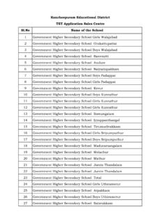
Kancheepuram Educational District TET Application …
trb.tn.nic.inSl.No Name of the School 28 Government Higher Secondary School Perunagar 29 Government Higher Secondary School Kammalampoondi 30 Government Higher Secondary School Manampathy

GOVERNMENT OF TAMIL NADU TEACHERS …
trb.tn.nic.inPaper ‐ I 3 PAPER1 GOVERNMENT OF TAMIL NADU TEACHERS RECRUITMENT BOARD 4th Floor, EVK Sampath Maaligai, DPI Compound, College Road, Chennai – 600 006. TAMIL NADU TEACHER ELIGIBILITY TEST (TNTET) – 2017 Paper - I PROSPECTUS Applications are invited for Teacher Eligibility Test, Paper I for the year …

GOVERNMENT OF TAMIL NADU TEACHERS …
trb.tn.nic.inPaper II 3 PAPER2 GOVERNMENT OF TAMIL NADU TEACHERS RECRUITMENT BOARD 4th Floor, EVK Sampath Maaligai, DPI Compound, College Road, Chennai – 600 006. TAMIL NADU TEACHER ELIGIBILITY TEST (TNTET) – 2017 Paper - II PROSPECTUS Applications are invited for Teacher Eligibility Test, Paper II for the …
Related documents
Chapter 1 Introduction to CMOS Circuit Design
www.ee.ncu.edu.twlogic that can be exploited in some CMOS designs ... static power Fully-restored logic (NMOS passes “0” only and ... Design Flow for a VLSI Chip Specification Behavioral Design Structural Design Physical Design Function Function Function Timing Power. Advanced Reliable Systems (ARES) Lab. Jin-Fu Li, EE, NCU 32 Circuit and System Representations

VLSI Design - Tutorialspoint
www.tutorialspoint.comprocessing power and portability. This trend is expected to grow rapidly, with very important implications on VLSI design and systems design. VLSI Design Flow The VLSI IC circuits design flow is shown in the figure below. The various levels of design are numbered and the blocks show processes in the design flow.

CS250 VLSI Systems Design Lecture 8: Memory
inst.eecs.berkeley.eduCS250 VLSI Systems Design Lecture 8: Memory John Wawrzynek, Krste Asanovic, with John Lazzaro and Yunsup Lee (TA) UC Berkeley Fall 2010. Lecture 8, Memory CS250, UC Berkeley, Fall 2010 CMOS Bistable Cross-coupled inverters used to hold state in CMOS “Static” storage in powered cell, no refresh needed ... Impacts power dissipation as ...

DRAM Design Overview - Stanford University
www.graphics.stanford.eduPower Supply Voltage (V) Active Power tRC=min. (A) Stand-by Power ( Low Power mode: mA) 4M 16M 64M 256M 1G 4G 10-2 10-1 100 101 Active Power VCC Low Power Stand-by Power Power Dissipation Trend Feb. 11th. 1998 DRAM Design Overview Junji Ogawa Refresh Specification Trend Numbers of Active S/As Refresh Cycles Refresh Interval (max.:ms)
LECTURE NOTES ON VLSI DESIGN B.Tech VII semester (R16)
www.iare.ac.innMOS process was less expensive than CMOS, nMOS logic gates still consumed power while idle. Power ... names would have to be created every five years if this naming trend continued and thus the term very large-scale integration (VLSI) is used to describe most integrated circuits from the 1980s onward. A corollary of
ECEN720: High-Speed Links Circuits and Systems Spring 2021
people.engr.tamu.eduResistor Options (90nm CMOS) Active Termination • Transistors must be used for ... driver power • Actualdriver power levels also depend on ... Upadhyaya, VLSI 2016. CML Driver w/ Higher Output Stage Supply 28 CK0 D CK90 Vbias VCC_HV VCC_NOM Vcs=~1V …
ECE 410: VLSI Design Course Lecture Notes
www.egr.msu.edu– power / transistor : decreasing with time (constant power density) – device channel length : decreasing with time – power supply voltage : decreasing with time ref: Kuo and Lou, Low-Voltage CMOS VLSI Circuits, Fig. 1.3, p. 3 transistors / chip power / transistor channel length supply voltage low power/ transistor is critical for future ICs

PSPICE Schematic Student 9.1 Tutorial
www1bpt.bridgeport.eduthe MOS transistors, generally in CMOS VLSI circuit schematic NMOS and PMOS are drawn as 3-terminal devices, as shown in the following figure. Figure. NMOS and PMOS symbols in CMOS VLSI schematics design ... power source). 6. After you placed all the parts, now your circuit should look like this. 6
Lecture 19: SRAM
user.engineering.uiowa.edu19: SRAM CMOS VLSI Design 4th Ed. 4 Array Architecture 2n words of 2m bits each If n >> m, fold by 2k into fewer rows of more columns Good regularity – easy to design Very high density if good cells are used