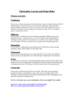
Fabrication, Layout and Design Rules
It is the process of depositing selected material such as Polysilicon, silicon dioxide, aluminum, cupper silicon nitride over the entire wafer Metalization Is the process of depositing metals on silicon dioxide over the entire wafer. Different metals and alloys are deposited in new chip fabrication, replacing the old aluminum.
Download Fabrication, Layout and Design Rules

Information
Domain:
Source:
Link to this page:
Documents from same domain

Introduction to Oracle WebLogic - Concordia …
users.encs.concordia.caIntroduction to Oracle WebLogic Presented by: FatnaBelqasmi, PhD, Researcher at Ericsson. Agenda • Overview • Download and installation • A concrete scenario using the real product • Hints for the project • Oracle WebLogic Web Server • Oracle Workshop for WebLogic Overview. Oracle WebLogicWeb Server

Material Handling - Concordia University
users.encs.concordia.caMaterial Handling Definitions Material handling is the combination of art and science of: moving storing protecting controlling the material Material handling means providing the right amount of the right material in the right condition
Project Report for COEN6511: ASIC Design
users.encs.concordia.ca2 Logic design for 4-bit comparator 2.1 logic design procedure Magnitude comparator is a combinational circuit that compares to numbers and determines their relative magnitude.
Mechanical Engineering Drawing - Concordia University
users.encs.concordia.caMECH 211, Mechanical Engineering Drawing ... Introduction to graphic language and design — means and techniques. The third and the first angle projections. Orthographic projection of points, lines, planes and solids. Principal and auxiliary views. Views in a given direction.
www.iop.org/journals/physed Gas turbine technology
users.encs.concordia.caRolls-Royce plc, Ansty, Coventry CV7 9JR, UK E-mail: peter.spittle@rolls-royce.com Abstract Gas turbine engines power most commercial flights operating today. Yet many people are ignorant of the cutting-edge technologies used in the creation and operation of …
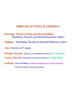
THREAD CUTTING & FORMING - Concordia University
users.encs.concordia.caTHREAD CUTTING & FORMING Threading, Thread Cutting and Thread Rolling: Machining Threads on External Diameters (shafts) ... - Blank material has Narrow tolerances for rolling. Only EXTERNAL THREADS can be ROLLED. USING OF FLAT DIES-The blank is rolled between two dies ... -Only external threads can be rolled-Only soft materials < HRC 37 can be ...
lecture 10 fracture students-2018.ppt - Concordia University
users.encs.concordia.caDr. M. Medraj Mech. Eng. Dept. – Concordia University MSE 521 Lecture 11/13 Cyclic Stresses • Range of stresses ( r) is the difference between max and min: r max min • Stress amplitude, a: 2 2 max min r
Material Handling - users.encs.concordia.ca
users.encs.concordia.caWrapping Stretch wrapping Shrink wrapping Unit load design Pallet Skids Stretch wrapping Shrink wrapping.

Tolerancing in ISO
users.encs.concordia.ca0.500 is the lower limit hole 0.496 is the upper limit shaft ... • Non-permanent fasteners – bolts and screws • Features, representation, assembly representation and note ... • Nominal size – in mm • Pitch size – in mm • General purpose tolerance – a tolerance ...
Mechanical Engineering Drawing
users.encs.concordia.caOrthographic projection of points, lines, planes and solids. Principal and auxiliary views. Views in a given direction. Sectional views. Intersection of lines, planes and solids. Development of surfaces. Drafting practices. Dimensioning, fits and tolerancing. Computer-aided drawing and solid modelling. Working drawings — detail and assembly ...
Related documents
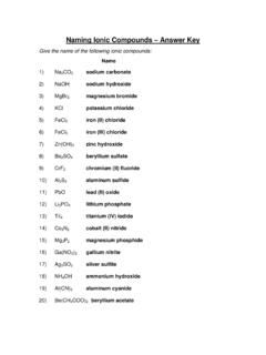
Naming Ionic Compounds – Answer Key - Weebly
siemianowski.weebly.com3N potassium nitride 7) SO 2 sulfur dioxide 8) CuOH copper(I) hydroxide 9) Zn(NO 2) 2 zinc nitrite 10) V 2S 3 vanadium(III) sulfide Write the formulas for the following chemical compounds: 11) silicon dioxide SiO 2 12) nickel (III) sulfide Ni 2S 3 13) manganese (II) phosphate Mn …
MEMS Fabrication I : Process Flows and Bulk Micromachining
www-bsac.eecs.berkeley.edu• Remove using solvents (acetone) or O 2 plasma ... • Silicon Dioxide, Silicon Nitride • Metals • Polymers Wolf and Tauber Silicon crystal structure λ= 5.43 Å ...

7. Polysilicon and Dielectric Film Deposition
www.cityu.edu.hkSilicon nitride is a barrier to sodium diffusion, is nearly impervious to moisture, and has a low oxidation rate. The local oxidation of silicon (LOCOS) process also uses silicon nitride as a mask. The patterned silicon nitride will prevent the underlying silicon from oxidation but leave the exposed silicon to be oxidized.

National 4XDOLÛFDWLRQV 208
chemistry-teaching-resources.com(c)Silicon tetrachloride can be used to make silicon nitride (Si 3N 4), a compound found in many cutting tools. (i) Silicon nitride has a melting point of 1900°C and does not conduct electricity when molten. Explain fully, in terms of structure and bonding, why silicon nitride has a …

BOE / HF – Silicon dioxide Etching Standard Operating ...
d1rkab7tlqy5f1.cloudfront.netJul 19, 2018 · This etch will remove silicon dioxide. It will only attack silicon and silicon nitride at a very slow rate. Some metals etch in BOE (Titanium, Aluminium) some do not (Chromium, Gold, Platinum). You can mask a BOE etch with photoresist for a short etch (20 mins or so). If you etch longer, the photoresist will start to peel off.

VLSI FABRICATION TECHNOLOGY
global.oup.comThis appendix will consider only silicon-based (Si) technologies. Although other compound materials in groups III through V, such as gallium arsenide (GaAs) and aluminum gallium nitride (AlGaN), are also used to implement VLSI chips, silicon is still the most popular material, with excellent cost–performance trade-off. Recent development in SiGe
MEMS Fabrication I : Process Flows and Bulk Micromachining
www-bsac.eecs.berkeley.edu• Remove using solvents (acetone) or O 2 plasma ... • Silicon Dioxide, Silicon Nitride • Metals • Polymers Wolf and Tauber Silicon crystal structure λ= 5.43 Å ...
Wet and Dry Etching - University of California, Davis
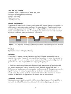
www.ece.ucdavis.eduSilicon dioxide or silicon nitride is usually used as a masking material against HNA. As the reaction takes place, the material is removed laterally at a rate similar to the speed of etching downward. This lateral and downward etching process takes places even with isotropic
Etch rates for micromachining processing-part II ...
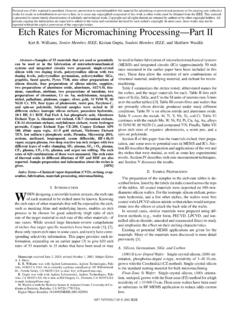
www.seas.upenn.eduWILLIAMS et al.: ETCH RATES FOR MICROMACHINING PROCESSING—PART II 765 TABLE IV ETCH RATES OF SILICON NITRIDE AND ALUMINUM OXIDE (nm/min) similar Borofloat glass) are used in anodic bonding to silicon due to the high content of mobile sodium ions and to the good match of thermal expansion rates.