NVIDIA TESLA V100 GPU ARCHITECTURE
to power the most computationally intensive HPC, AI, and graphics workloads. The GV100 GPU includes 21.1 billion transistors with a die size of 815 mm2. It is fabricated on a new TSMC 12 nm FFN (FinFET NVIDIA) high-performance manufacturing process customized for NVIDIA.
Download NVIDIA TESLA V100 GPU ARCHITECTURE

Information
Domain:
Source:
Link to this page:
Documents from same domain
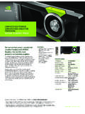
uNMatChed PoWer. uNMatChed CreatIVe NVIdIa …
images.nvidia.comTitle: Data Sheet: Quadro P5000 Author: NVIDIA Corporation. Subject: NVIDIA® QUADRO® P5000, 16GB GDDR5X, CUDA, GRAPHICS Created Date: 9/12/2016 2:17:53 PM

NVIDIA GRID SOFTWARE SERVICE SUPPLEMENTAL TERMS YI TP
images.nvidia.coma) When You purchase a Service Subscription plan for a certain NVIDIA Software, all of Your licenses to such NVIDIA Software must be enrolled in the same Service Subscription plan. b) NVIDIA is not obligated to provide any Service to You if such Service is no longer made generally

THE QUESTION - images.nvidia.com
images.nvidia.comAutoCAD 2015. These metrics are based on tests with the lab equipment shown in the graphic below, using the Cadalyst benchmark, and in working with Autodesk and their emphasis on end user usability. Of course, your usage will depend on your models and

GONE GIRL PRODUCTION BUILDS FIRST 6K FEATURE FILM ... - …
images.nvidia.comThe production system and workflow for Gone Girl is the most advanced technical design of any feature film to date. The filmmakers opted to shoot in 6K, but frame for 5K to have an ability to reframe and stabilize, with greater resolution than before. They also wanted to retain control

GPU accelerated Datacenter for Smart Cities - Nvidia
images.nvidia.comGPU accelerated Datacenter for Smart Cities. City Challenges ... self-sustainable framework Bring together certified ecosystem partners Create a citywide Wi-Fi network ... infrastructure based on Cisco wireless solutions Increased City Center’s appeal by offering free, fast Wi-Fi
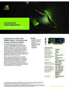
ACCeLerAte Your CreAtIVItY NVIDIA QuADro K620
images.nvidia.comNVIDIA QuADro K620 | DAtA Sheet | MAr16 1 Via supplied adapter/connector/bracket | 2 Windows 7, 8, 8.1 and Linux | 3 Product is based on a published Khronos Specification, and is expected to pass the Khronos Conformance Testing Process when available. Current conformance status can be found at

TESLA M60 - Nvidia
images.nvidia.comgraphics processing units (GPUs). The Tesla M60 has 16 GB GDDR5 memory (8 GB per GPU) and a 300 W maximum power limit. The board is offered in a 300 W passively cooled variant that requires system airflow to properly

End to End Learning for Self-Driving Cars - Nvidia
images.nvidia.comEnd to End Learning for Self-Driving Cars Mariusz Bojarski NVIDIA Corporation Holmdel, NJ 07735 Davide Del Testa NVIDIA Corporation Holmdel, NJ 07735
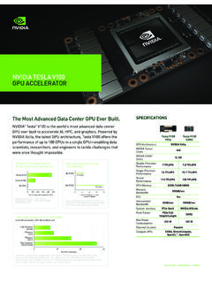
NVIDIA TESLA V100 GPU ACCELERATOR
images.nvidia.comNVIDIA TESLA V100 GPU ACCELERATOR The Most Advanced Data Center GPU Ever Built. NVIDIA® Tesla® V100 is the world’s most advanced data center GPU ever built to accelerate AI, HPC, and graphics. Powered by
Featuring Pascal GP100, the World’s Fastest GPU
images.nvidia.comsystems. The ratio of GPUs to CPUs has also increased. 2012’s fastest supercomputer, the Titan located at Oak Ridge National Labs, deployed one GK110 GPU per CPU. Today, two or more GPUs are more commonly being paired per CPU as developers increasingly expose and leverage the available parallelism provided by GPUs in their applications.
Related documents
Fundamentals of Computer Aided Design
www.pages.drexel.eduDept of Mechanical Engineering and Mechanics, Drexel University Dimensions • A dimension is for size and position (of the designed/modeled shape). •A DIMENSION is a numerical value expressed in appropriate units of measurement and used to define the size, location, orientation, form

DRAM Design Overview - Computer Graphics at Stanford ...
www.graphics.stanford.eduDRAM Design Overview Junji Ogawa 90 92 94 96 98 00 02 04 06 08 10 1000 100 20 50 200 500 64M 256M 1G Die Size(mm2) Early Production 256M Production 1G 4G 0.35 0.18 0.13 0.10 Rule (um) Year i-line ArF ? 16M 0.50 64M 0.25 4G KrF 128M KrF+α Standard DRAM Development Conference Feb. 11th. 1998 DRAM Design Overview Junji Ogawa Bit Cost Trend of ...

NVIDIA TESLA P40 GPU ACCELERATOR
www.nvidia.comenabling professional and design engineering workflows at peak performance. The Tesla P40 delivers up to 2X the graphics performance compared to the M60 (Refer to Performance Graph). Users can count on consistent performance with the new resource scheduler, which provides deterministic QoS and eliminates the problem of a “noisy neighbor.”

Datasheet Quadro M2000 - Nvidia
www.nvidia.comadvanced graphics card features an NVIDIA Maxwell™-based GPU, plus 4 GB of ultra-fast on-board memory and the power to drive four 4K displays natively. This makes it an excellent choice for accelerating product development and content creation workflows that demand fluid interactivity with complex models and scenes.