
TN-46-05 GENERAL DDR SDRAM FUNCTIONALITY …
overview of the 2 n-prefetch architecture, a strobe-based data bus, and the SSTL_2 interface used with DDR SDRAM. It will also highlight the functional differences between SDR and the improved DDR memory technol-ogy. For detailed design and timing criteria for DDR ... DON’T CARE (to DRAM) DON'T CARE (to controller) NOTES: 1.
Download TN-46-05 GENERAL DDR SDRAM FUNCTIONALITY …

Information
Domain:
Source:
Link to this page:
Documents from same domain

Micron Serial NOR Flash Memory
www.micron.comMicron Serial NOR Flash Memory 3V, Multiple I/O, 4KB, 32KB, 64KB, Sector Erase MT25QL128ABA Features • SPI-compatible serial bus interface • Single and double transfer rate (STR/DTR)
TN-40-07: Calculating Memory Power for DDR4 SDRAM
www.micron.comThis technical note details how DDR4 SDRAM consumes power and provides the tools ... TN-40-07: Calculating Memory Power for DDR4 SDRAM Introduction CCM005-524338224-10497 Rev. B 8/18 EN 1 ... (XXX), where XXX is the subcomponent power.) 2. Derate the power based on the command scheduling in the system (Psch[XXX]).
2Gb NAND Flash Memory - Micron Technology
www.micron.com2, 4, 8Gb: x8/x16 Multiplexed NAND Flash Memory List of Figures PDF: 09005aef818a56a7 / Source: 09005aef81590bdd Micron Technology, Inc., reserves the right to change products or specifications without notice.

TN-ED-03: GDDR6: The Next-Generation Graphics DRAM
www.micron.comFrom the figure above it becomes apparent that the three GDDR standards have many similarities. In fact, taking GDDR5 as the parent GDDR standard, only select items have been modified from the migration of GDDR5 to GDDR5X and GDDR6 to allow as smooth a transition as possible to each next-generation standard.
Micron Serial NOR Flash Memory
www.micron.comMicron Serial NOR Flash Memory 3V, Multiple I/O, 4KB Sector Erase N25Q256A Features • SPI-compatible serial bus interface • Double transfer rate (DTR) mode • 2.7–3.6V single supply voltage • 108 MHz (MAX) clock frequency supported for all protocols in single transfer rate (STR) mode • 54 MHz (MAX) clock frequency supported for all

TN-41-02: DDR3 ZQ Calibration
www.micron.comTechnical Note DDR3 ZQ Calibration Introduction For more robust system operation, the DDR3 SDRAM driver design has been enhanced with reduced capacitance, dynamic on-die termination (ODT), and a new calibration scheme. The capacitance reduction comes from the use of a new “merged” driver. With

Introduction Technical Note - Micron Technology
www.micron.comIntroduction PDF: 09005aef8467c543/Souce: 09005aef8467d772 Micron Technology, Inc., reserves the right to change products or specifications without notice. tn2959_bbm_in_nand_flash.fm - Rev. H 4/11 EN 1 ©2011 Micron Technology, Inc.

TN-41-13: DDR3 Point-to-Point Design Support
www.micron.comVoltage (core, I/O) 1.8V 1.5V Lower power Low power (core, I/O) NA 1.35V Lower power VREF input 1 – all inputs 2 – DQs and CMD/ADDR Improved power delivery Data rate 800 MT/s 1600 MT/s 2X data rate tCK DLL enabled 125–400 MHz 300–800 MHz 2X clock rate tCK DLL disabled Undefined 12.8–125 MHz Slow clock debug Prefetch 4 bits (4n) 8 bits ...

TN-ED-04: GDDR6 Design Guide - Micron Technology
www.micron.comsignal is such that it is always sourced from DRAM to controller, for both reads and writes. Due to this, extra care is recommended during PCB design and analysis ensuring the EDC net is evaluated for both near-end and far-end crosstalk. TN-ED-04: GDDR6 Design Guide GDDR6 Overview CCM005-524338224-10517 tn_ed_04_gddr6_design_guide.pdf - Rev. B ...
Hybrid Memory Cube HMC Gen2 - Micron Technology
www.micron.comHybrid Memory Cube (HMC) is a single package con-taining four DRAM die and one logic die, all stacked together using through-silicon via (TSV) technology. Within each cube, memory is organized vertically— portions of each memory die are combined with the corresponding portions of the other memory die in the stack.
Related documents
DRAM Technology - Smithsonian Institution
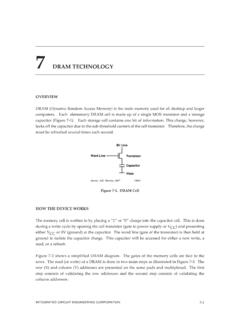
smithsonianchips.si.eduOVERVIEW DRAM (Dynamic Random Access Memory) is the main memory used for all desktop and larger computers. Each elementary DRAM cell is made up of a single MOS transistor and a storage capacitor (Figure 7-1). Each storage cell contains one bit of information. This charge, however,

DRAM Design Overview - Stanford University
www.graphics.stanford.eduDRAM Design Overview Junji Ogawa ASSP/ASIC Standard Operating Frequency Customizability WRAM VRAM DRAM/Logi c SLDRAM CDRAM EDRAM EDO MDRAM Function rich DRAM 100MHz 200MHz 500MHz DDR 1GHz 2GHz High-speed DRAM Target SDRAM RAMBUS DRAM Operating Frequency v.s. Customizability Feb. 11th. 1998 DRAM Design …

Understanding DRAM Operation
compas.cs.stonybrook.eduUnderstanding DRAM Operation 12/96 Page 1 Overview Dynamic Random Access Memory (DRAM) devices are used in a wide range of electronics applications. Although they are produced in many sizes and sold in a variety of packages, their overall operation is essentially the same. DRAMs are designed for the sole purpose of storing data.

For the year ended December - Samsung us
images.samsung.comDS DRAM, NAND flash, mobile APs, OLED panels for smartphones, etc. Harman Digital cockpits, telematics, speakers, etc. SEC is a global electronics firm comprising the headquarters in Korea and 241 subsidiaries (collectively, “Samsung ... Businesses Overview』, for …
SAMSUNG ELECTRONICS Co., Ltd. 2019 BusinessReport
images.samsung.comBusiness Overview』. Samsung Electronics Business Report 2 / 261 Table of Contents ... brains of mobi le products—and with memory components like DRAM via enhanced capacity and density. The Memory Business its position has maintained at the top of the global memory market by sustaining cost

Highlights of the High- Bandwidth Memory (HBM) Standard
www.cs.utah.eduJun 14, 2014 · HBM Overview Standard defines an HBM stack Bonding footprint Interface Signaling Commands & Protocol Some optional features: ECC support Base-layer logic/redistribution/IO die Standard does not define Internal architecture of the stack Precise DRAM timing parameters . The Memory Forum – June 14, 2014 HBM Overview Each HBM …

Memory Basics - Michigan State University
www.egr.msu.eduMemory Overview.4 Comparison of Memory Types •DRAM – very high density cheap data cache in computers – must be periodically refreshed slower than SRAM – volatile; no good for program (long term) storage •SRAM(basically a Latch) – fastest type of memory yt i …
TN-40-40: DDR4 Point-to-Point Design Guide - Micron …
www.micron.comDDR4 Overview DDR4 SDRAM is a high-speed dynamic random-access memory internally configured as an 8-bank DRAM for the x16 configuration and as a 16-bank DRAM for the x4 and x8 configurations. The device uses an 8n-prefetch architecture to achieve high-speed oper-ation. The 8n-prefetch architecture is combined with an interface designed to transfer