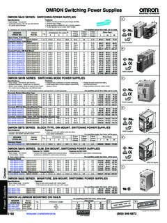
Transcription of TN15 SPI Interface Specification - Mouser
1 Technical Note 15 1(5) SPI Interface Specification OBJECTIVE This document specifies the Serial Peripheral Interface (SPI) that is used in the SCA61T, SCA100T, SCA103T, SCA1000, and SCA1020 series sensors. THE SPI Interface A Serial Peripheral Interface (SPI) system consists of one master device and one or more slave devices. The master is defined as a microcontroller providing the SPI clock and the slave as any integrated circuit receiving the SPI clock from the master. The ASIC in VTI Technologies products always operates as a slave device in master-slave operation mode. The SPI has a 4-wire synchronous serial Interface . Data communication is enabled with a low active Slave Select or Chip Select wire (CSB).
2 Data is transmitted with a 3-wire Interface consisting of wires for serial data input (MOSI), serial data output (MISO) and serial clock (SCK). DATA OUT (MOSI)DATA IN (MISO)SERIAL CLOCK (SCK)SS0SS1SS2SS3 MASTERMICROCONTROLLERSISOSCKCSSLAVESISOS CKCSSISOSCKCSSISOSCKCS Figure 1. Typical SPI connection The SPI Interface in VTI products is designed to support any microcontroller that uses SPI bus. communication can be carried out by software or hardware based SPI. Please note that in the case of hardware based SPI, the received acceleration data is 11 bits. The SPI Interface is used for testing and calibration purposes, and it can also be used in the final application.
3 Some of the test and calibration commands are disabled in normal use, and are not documented here. The data transfer uses the following 4-wire Interface : MOSI master out slave in P ASIC MISO master in slave out ASIC P SCK serial clock P ASIC CSB chip select (low active) P ASIC 19 Sep 2005 VTI Technologies reserves all rights to modify this document without prior notice. Technical Note 15 2(5) Each transmission starts with a falling edge of CSB and ends with the rising edge. During transmission, commands and data are controlled by SCK and CSB according to the following rules: commands and data are shifted; MSB first, LSB last each output data/status bits are shifted out on the falling edge of SCK (MISO line) each bit is sampled on the rising edge of SCK (MOSI line) after the device is selected with the falling edge of CSB, an 8-bit command is received.
4 The command defines the operations to be performed the rising edge of CSB ends all data transfer and resets internal counter and command register if an invalid command is received, no data is shifted into the chip and the MISO remains in high impedance state until the falling edge of CSB. This reinitializes the serial communication . In order to perform other commands than those listed in Table 1, the lock register content must be set correctly. If such a command is fed without setting the correct lock register content, no data will be shifted into the chip and the MISO remains in high impedance state until the falling edge of CSB. data transfer to MOSI continues immediately after receiving the command in all cases where data is to be written to ASIC s internal registers data transfer out from MISO starts with the falling edge of SCK immediately after the last bit of the SPI command is sampled in on the rising edge of SCK maximum SPI clock frequency is 500kHz maximum data transfer speed for RDAX and RDAY is 6600 samples per sec / channel SPI command can be either an individual command or a combination of command and data.
5 In the case of combined command and data, the input data follows uninterruptedly the SPI command and the output data is shifted out parallel with the input data. 7654321076543210 CSBSCKMISOMOSI0123456789101112131415 HIGH IMPEDANCECOMMANDDATA INDATA OUT Figure 2. Command and data transmission over the SPI After power up, the circuit starts to operate in Measure mode. This is the normal operation mode that is used for the applications. 19 Sep 2005 VTI Technologies reserves all rights to modify this document prior notice. Technical Note 15 3(5) DIGITAL Interface Specification (TABLE 1) Parameter Condition Min Typ Max Units Digital output load @ 500 kHz 1 nF SPI clock frequency (1 500 kHz Internal AD conversion 150 s Data transfer time @ 500 kHz 38 s Note1.)
6 Minimum SPI frequency depends on the master microcontroller clock frequency THE SPI COMMANDS The SPI Interface uses an 8-bit instruction (or command) register. The list of commands is given in Table 2. Table 2. SPI commands. The commands in Italic are in use in the 2-axis SCA100T only. Command Command format Description: MEAS 00000000 Measure mode (normal operation mode after power on) RWTR 00001000 Read and write temperature data register STX 00001110 Activate Self test for X-channel STY 00001111 Activate Self test for Y-channel RDAX 00010000 Read X-channel acceleration through SPI RDAY 00010001 Read Y-channel acceleration through SPI Measure mode (MEAS) is standard operation mode after power-up. During normal operation, MEAS command is the exit command from Self test.
7 Read temperature data register (RWTR) reads temperature data register during normal operation without effecting the operation. Temperature data register is updated every 150 s. The load operation is disabled whenever the CSB signal is low, hence CSB must stay high at least 150 s prior the RWTR command in order to guarantee correct data. The data transfer is presented in Figure 3, and the data is transferred MSB first. In normal operation, it does not matter what data is written into temperature data register during the RWTR command and hence writing all zeros is recommended. Self test for X-channel (STX) activates the self test function for the X-channel (Channel 1).
8 The Internal charge pump is activated and a high voltage is applied to the X-channel acceleration sensor element electrode. This causes the electrostatic force that deflects the beam of the sensing element and simulates the acceleration to the positive direction. The X-channel self-test is de-activated by giving the MEAS command. Self test for Y-channel (STY) activates the self test function for the Y-channel (Channel 2). The internal charge pump is activated and a high voltage is applied to the Y-channel acceleration sensor element electrode. This causes the electrostatic force that deflects the beam of the sensing element and simulates the acceleration to the positive direction.
9 The Y-channel self-test is de-activated by giving the MEAS command. Note! This command is valid for the 2-axis SCA100T only. Read X-channel acceleration (RDAX) accesses the AD converted X-channel (Channel 1) acceleration signal stored in acceleration data register X. During normal operation, acceleration data register X is reloaded every 150 s. The load operation is disabled whenever the CSB signal is low, hence CSB must stay high at least 150 s prior the RDAX command in order to guarantee correct data. Data output is an 11-bit digital word that is fed out MSB first and LSB last. (see Figures 3 and 4). 19 Sep 2005 VTI Technologies reserves all rights to modify this document without prior notice.
10 Technical Note 15 4(5) Read Y-channel acceleration (RDAY) accesses the AD converted Y-channel (Channel 2) acceleration signal stored in acceleration data register Y. During normal operation acceleration data register Y is reloaded every 150 s. The load operation is disabled whenever the CSB signal is low, hence CSB must stay high at least 150 s prior the RDAY command in order to guarantee correct data. Data output is an 11-bit digital word that is fed out MSB first and LSB last. Note! This command is valid for the 2-axis SCA100T only. RDAX COMMAND AND DATA TRANSMISSION OVER THE SPI (FIGURE 3) MSB MISO in high-impedance during 8-bit command.