Transcription of Crack detection and analyses using resonance …
1 Crack detection and analyses using resonance ultrasonic vibrationsin full-size crystalline silicon wafersA. Belyaev, O. Polupan, W. Dallas, S. Ostapenko,a and D. HessNanomaterials and Nanomanufacturing Research Center, University of South Florida, 4202 East FowlerAvenue, Tampa, Florida 33620J. WohlgemuthBP Solar International LLC, Frederick, Maryland 21703 Received 13 April 2005; accepted 8 February 2006; published online 15 March 2006 An experimental approach for fast Crack detection and length determination in full-size solar-gradecrystalline silicon wafers using a resonance ultrasonic vibrations RUV technique is presented. TheRUV method is based on excitation of the longitudinal ultrasonic vibrations in full-size an external piezoelectric transducer combined with a high sensitivity ultrasonic probe andcomputer controlled data acquisition system, real-time frequency response analysis can beaccomplished. On a set of identical crystalline Si wafers with artificially introduced peripherycracks, it was demonstrated that the Crack results in a frequency shift in a selected RUV peak to alower frequency and increases the resonance peak bandwidth.
2 Both characteristics were found toincrease with the length of the Crack . The frequency shift and bandwidth increase serve as reliableindicators of the Crack appearance in silicon wafers and are suitable for mechanical quality controland fast wafer inspection. 2006 American Institute of Physics. The photovoltaic industry, with crystalline silicon as adominant segment, is expanding rapidly to meet growing re-newable energy demands all over the world. One of the cur-rent technological problems is to identify and eliminatesources of mechanical defects such as thermo-elastic stressand cracks leading to the loss of wafer integrity and ultimatebreakage of as-grown and processed Si wafers and cells. Theproblem is of increased concern as a result of the currentstrategy of reducing wafer thickness down to 100 generated during wafer sawing or laser cutting canpropagate due to wafer handling and solar cell processing , phosphorous diffusion, antireflecting coating, front andback contact firing, and soldering of contact grid.
3 It is rec-ognized that development of a methodology for fast in-linecrack detection and control is required to match the through-put of typical production lines. At this time, there are severalexperimental methods, which address the problem of crackdetection in silicon. They include scanning acousticmicroscopy,2ultrasonic lock-in thermography,3and millime-ter wave Crack can be also accessed usinglaser-induced ultrasonic of these methods aresuitable in their present form for rapid in-line Crack diagnos-tics of as-grown and processed Si wafers. In solar cell manu-facturing, in-line control requires methods which can achievemeasurement times close to 2 s/wafer to match a throughputof a production this letter, we propose utilizing an alternative ap-proach based on the recently developed resonance ultrasonicvibrations RUV methodology, which was successfully ap-plied to monitor elastic stress in multicrystalline siliconsolar-grade the RUV method, ultrasonic vibrations of a tunablefrequency and adjustable amplitude are applied to the siliconwafer.
4 ultrasonic vibrations are generated in the wafer usingan external piezoelectric transducer in the frequency rangefrom 20 to 90 kHz. The transducer contains a central holeallowing a reliable vacuum coupling between the wafer andtransducer by applying a small 50 kPa negative pressureto the backside of the wafer. The vibrations propagate intothe wafer from the transducer and form standing acousticwaves at resonance frequencies, which can be analyzed witha broadband ultrasonic probe. using a frequency sweep f-scan through a particular resonance mode, the RUV sys-tem provides accurate measurements of the resonance fre-quency, the maximum vibration amplitude, and the band-width BW of the resonance curve using the ultrasonicprobe. In the present design, the broadband ultrasonic probemeasures the longitudinal vibration mode characteristics bycontacting the edge of the wafer with a sensor controlledcontact force. The ac signal from the probe is measured us-ing standard lock-in technique andf-scans are analyzed byWINDOWS based software.
5 The system is described in moredetails also used theHS1000 HiSPEEDTM scanning acoustic microscope SAM by Sonix Inc. for sur-face morphology and structural bulk integrity evaluation ofthe set of 20 identical 125 mm 125 mm pseudosquareshaped 100 oriented Czochralski silicon Cz-Si waferswere chosen for this study. This shape represents one of theaccepted photovoltaic industry standards. The wafers wereas-grown with a nominal thickness of cm. All waferswere initially screened by SAM for structural integrity. TheSAM maps have been measured with a 100 m step and noperiphery or bulk cracks have been observed within this ac-curacy. using the RUV vibrations technique frequency scansof the longitudinal vibrations from 20 to 85 kHz were mea-sured on all wafers. A typical full range acoustic spectrumobtained on one of the wafers is shown in Fig. 1. In thefrequency spectrum, we observed a set of distinctive reso-nance modes, which are consistently reproduced from waferto wafer in terms of the maximum amplitude 10% , fre-a Author to whom correspondence should be addressed; electronic PHYSICS LETTERS88, 111907 2006 0003-6951/2006/88 11 /111907/3/$ 2006 American Institute of Physics88, 111907-1 Downloaded 13 Apr 2006 to Redistribution subject to AIP license or copyright, see position 10 Hz and BW 10 Hz.
6 One of theseresonance modes assigned hereafter theAmode is observedat frequencyf=49 930 20 Hz. We suggest trackingf-scancharacteristics of theAmode as a means of Crack detectionand control in the wafers. A primary criterion for theA-modeselection is a noticeable clearance from the neighbor peaks toavoid their overlapping and interference, which would re-duce the accuracy of the mode analyses . As seen from Fig. 1 inset , theAmode is indeed a standalone narrow peak withBW=90 10 emphasize that theA-mode frequency scan andshape analyses can be measured with sufficient signal-to-noise ratio 20 dB in a time as short as 3 s. This obviouslymakes the RUV approach feasible and attractive for potentialimplementation as an in-line wafer quality control other important feature of the RUV method is that ac-cording to vibration theory, the resonance frequencies of thelongitudinal vibration modes are independent of the waferthickness h , in contrast to the flexural vibrations, which areproportional toh3 is especially beneficial in the mul-ticrystalline silicon mc-Si ribbon wafers, which may havesignificant up to 20% thickness variations across the wafer,as well as from wafer to wafer, which can be measured ac-curately using the SAM tested this statementby varying the Cz-Si wafer s thickness between 100 and350 m.
7 The frequency of the principle vibration modes ob-served in the RUV scans show slight high-frequencyshift with reduced wafer thickness, which can be attributedto stress increase as was previously observed in mc-Si should be noted that every resonant peak shown inFig. 1 represents a certain longitudinal vibration mode, bothsymmetrical and asymmetrical. Other type of vibrations , flexural modes has lower frequencies and has to beexcited in a different ,10In this letter, we concentrateon theAmode only. The solid line in the insert in Fig. 1shows the numeric approximation of the experimental fre-quency sweep for theAmode. This approximation is ob-tained with the Lorentz function and the following param-eters have been extracted: peak resonance frequency,f0, andbandwidth, introduce or engineer cracks with different sizes, wehave taken a few wafers and formed the Crack by scribing thewafer edge with a diamond pin. As expected, the cracksoriginate at the spot of the diamond application and are ori-ented along 110 crystallographic directions.
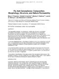
8 The length ofeach engineered Crack has been measured using SAM in theprecision mode with a 10 m step. The SAM image of oneof these cracks is presented in Fig. 2 a . After careful SAMstudy, the RUV measurements on the wafers with crackshave been carried out and the frequency spectra of theAmode recorded. In Fig. 3, we demonstrate theA-mode spec-tra in wafers with different Crack sizes. Clearly, theA-moderesonance frequency decreases with increasing Crack length also see fline in inset in Fig. 3 . We noticed that thevibration spectrum of the wafer with the 28 mm Crack isnonsymmetrical indicating sufficient nonlinearity of the wa-fer vibrations induced by the Crack . In addition, theA-modeBW increases with Crack length. We were able to clearlydetect mm size cracks by assessingA-mode line shift andbroadening. Specifically, a 3 mm Crack is exhibited as160 Hz shift and an 8% increase BW. We estimate that theRUV approach offers submillimeter Crack length sensitivityin Cz-Si downward shift with Crack length of the low-frequency flexural resonance modes was previously observedin circular shaped decrease of theA-modefrequency and its dependence on Crack length observed inour study are consistent with finite element analysis FEA.
9 12 The wafer is modeled as a 125 125 mesh, with the size ofFIG. 1. Full range ultrasonic frequency spectrum obtained on 125 mm 125 mm Cz-Si wafer. Inset shows theA-mode experimental data opencircles and fitting Lorentz approximation solid line . Line bandwidth BW parameter is shown by 2. a Scanning Acoustic Microscopy image of the 125 mm 125 mm Cz-Si wafer with introduced 28 mm periphery Crack . b Vibra-tion mode at 51 052 Hz obtained with finite element analysis calculations onthe wafer with identical Crack . The color bar represents relative values of theacoustic amplitude of the Phys. , 111907 2006 Downloaded 13 Apr 2006 to Redistribution subject to AIP license or copyright, see elements being mm mm. The pseu-dosquare wafers are modeled with isotropic eight-node pla-nar elements with a Young s modulus of 167 GPa, a Pois-son s coefficient of , and a density of 103 resonance frequencies up to 100 kHz and respectivemode shapes of the free edge longitudinal vibrations of theshell were calculated.
10 We concentrated on the frequency shiftof the vibration mode atf0=51 052 Hz, which is closest tothe experiment value for theAmode. Figure 2 b shows acalculated profile of the vibration mode on the wafer withidentical geometry as the experimental Cz-Si wafers contain-ing a 28 mm periphery Crack . The Crack size and location areidentical to the experimental values. The FEA shows a de-crease in frequency shift with increased Crack length, whichsupports our experiment. However, calculated values show amuch larger frequency shift than observed , in a case of 28 mm Crack FEA predicts a shift oftheA-mode peak at 6900 Hz experimental data is f=2 450 Hz . It was initially thought that one possibility forthis difference could be the increase in damping in the testwafers with increased Crack length. However, even thoughthe BW is proportional to damping, and therefore dampingincreases with Crack length by about 1 order of magnitude inthe tests presented, the actual damping levels associated withthe longitudinalAmode are very low for all test , the increased damping with Crack length does notnotably decrease the modal frequency.