Transcription of Ö OUT 6 OUT 7 IS31FL3218 18 CHANNELS LED …
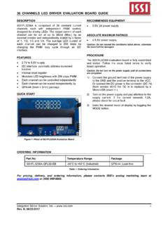
1 IS31FL3218 . 18 CHANNELS LED DRIVER. September 2016. GENERAL DESCRIPTION FEATURES. IS31FL3218 is comprised of 18 constant current to supply CHANNELS each with independent PWM control, I2C interface, automatic address increment designed for driving LEDs. The output current of each function channel can be set at up to 38mA (Max.) by an external Internal reset register resistor. The average LED current of each channel can Modulate LED brightness with 256 steps PWM. be changed in 256 steps by changing the PWM duty cycle through an I2C interface. Each channel can be controlled independently -40 C to +85 C temperature range The chip can be turned off by pulling the SDB pin low or QFN-24 (4mm 4mm), SOP-24 package by using the software shutdown feature to reduce power consumption.
2 The slave address is fixed 1010. 1000 . IS31FL3218 is available in QFN-24 (4mm 4mm) and APPLICATIONS. SOP-24. It operates from to over the Mobile phones and other hand-held devices for temperature range of -40 C to +85 C. LED display LED in home appliances TYPICAL APPLICATION CIRCUIT. VBattery VBattery 7. 3 OUT1. VCC 8. OUT2. 1 F F 9. OUT3. 10. OUT4. 11. OUT5. VDD 12. OUT6. 13. OUT7. 14. 5. IS31FL3218 OUT8. 15. SDA OUT9. Micro 6 16. SCL OUT10. Controller 24 17. SDB OUT11. 18. 100k OUT12. 19. OUT13. 20. OUT14. 21. 2 OUT15. R_EXT 22. OUT16. 23. 4 OUT17. GND 1. OUT18. Figure 1 Typical Application Circuit Note: The maximum output current is set up to 23mA when REXT =.
3 The maximum output current can be set by external resistor, R EXT. Please refer to the detail information in Page 9. Note: The IC should be placed far away from the mobile antenna in order to prevent the EMI. Integrated Silicon Solution, Inc. 1. Rev. D, 09/02/2016. IS31FL3218 . PIN CONFIGURATION. Package Pin Configuration (Top View). 23 OUT17. 22 OUT16. 21 OUT15. 20 OUT14. 19 OUT13. 24 SDB. OUT18 1 18 OUT12. R_EXT 2 17 OUT11. VCC 3 16 OUT10. QFN-24. GND 4 15 OUT9. SDA 5 14 OUT8. SCL 6 13 OUT7. OUT4 10. OUT5 11. OUT6 12. OUT1 7. OUT2 8. OUT3 9. OUT18 1 24 SDB. R_EXT 2 23 OUT17.
4 VCC 3 22 OUT16. GND 4 21 OUT15. SDA 5 20 OUT14. SCL 6 19 OUT13. SOP-24. OUT1 7 18 OUT12. OUT2 8 17 OUT11. OUT3 9 16 OUT10. OUT4 10 15 OUT9. OUT5 11 14 OUT8. OUT6 12 13 OUT7. PIN DESCRIPTION. No. Pin Description 1 OUT18 Output channel for LEDs. Input terminal used to connect an external resistor. 2 R_EXT. This regulates the output current. 3 VCC Power supply. 4 GND Ground. 5 SDA I2C serial data. 6 SCL I2C serial clock. 7~23 OUT1 ~ OUT17 Output channel for LEDs. 24 SDB Shutdown the chip when pulled low. Thermal Pad Connect to GND. Integrated Silicon Solution, Inc. 2. Rev. D, 09/02/2016.
5 IS31FL3218 . ORDERING INFORMATION. Industrial Range: -40 C to +85 C. Order Part No. Package QTY. IS31FL3218 -QFLS2-TR QFN-24, Lead-free 2500/Reel IS31FL3218 -GRLS2 SOP-24, Lead-free 30/Tube Copyright 2016 Integrated Silicon Solution, Inc. All rights reserved. ISSI reserves the right to make changes to this specification and its products at any time without notice. ISSI assumes no liability arising out of the application or use of any information, products or services described herein. Customers are advised to obtain the latest version of this device specification before relying on any published information and before placing orders for products.
6 Integrated Silicon Solution, Inc. does not recommend the use of any of its products in life support applications where the failure or malfunction of the product can reasonably be expected to cause failure of the life support system or to significantly affect its safety or effectiveness. Products are not authorized for use in such applications unless Integrated Silicon Solution, Inc. receives written assurance to its satisfaction, that: a.) the risk of injury or damage has been minimized;. b.) the user assume all such risks; and c.) potential liability of Integrated Silicon Solution, Inc is adequately protected under the circumstances Integrated Silicon Solution, Inc.
7 3. Rev. D, 09/02/2016. IS31FL3218 . ABSOLUTE MAXIMUM RATINGS. Supply voltage, VCC ~ + Voltage at SCL, SDA, SDB, OUT1 ~ OUT18 ~ VCC+ Maximum junction temperature, TJMAX 150 C. Storage temperature range, TSTG -65 C ~ +150 C. Operating temperature range, TA 40 C ~ +85 C. Thermal resistance, junction to ambient, JA(QFN) C /W. JA (SOP) C /W. ESD (HBM) 4kV. ESD (CDM) 1kV. Note: Stresses beyond those listed under Absolute Maximum Ratings may cause permanent damage to the device. These are stress ratings only and functional operation of the device at these or any other condition beyond those indicated in the operational sections of the specifications is not implied.
8 Exposure to absolute maximum rating conditions for extended periods may affect device reliability. ELECTRICAL CHARACTERISTICS. TA = -40 C ~ +85 C, VCC = ~ , unless otherwise noted. Typical values are TA = 25 C, VCC = Symbol Parameter Condition Min. Typ. Max. Unit VCC Supply voltage V. Maximum output current of VCC = , VOUT = IMAX 38 mA. each channel REXT = 2k (Note 1). ICC Quiescent power supply current REXT = mA. ISD Shutdown current VSDB = 0V or software shutdown A. VSDB = 0V or software shutdown, IOZ Output leakage current 1 A. VOUT = 5V. VEXT Output voltage of R-EXT pin V.
9 Logic Electrical Characteristics (SDA, SCL, SDB). VIL Logic 0 input voltage VCC = V. VIH Logic 1 input voltage VCC = V. 5. IIL Logic 0 input current nA. (Note 2). 5. IIH Logic 1 input current nA. (Note 2). Integrated Silicon Solution, Inc. 4. Rev. D, 09/02/2016. IS31FL3218 . DIGITAL INPUT SWITCHING CHARACTERISTICS (Note 2). Symbol Parameter Condition Min. Typ. Max. Unit fSCL Serial-Clock frequency 400 kHz Bus free time between a STOP and a START. tBUF s condition tHD, STA Hold time (repeated) START condition s tSU, STA Repeated START condition setup time s tSU, STO STOP condition setup time s tHD, DAT Data hold time s tSU, DAT Data setup time 100 ns tLOW SCL clock low period s tHIGH SCL clock high period s Rise time of both SDA and SCL signals, tR (Note 3) 20+ 300 ns receiving Fall time of both SDA and SCL signals, tF (Note 3) 20+ 300 ns receiving Note 1: The recommended minimum value of REXT is 2k , or it may cause a large current.
10 Note 2: Guaranteed by design. Note 3: Cb = total capacitance of one bus line in pF. ISINK 6mA. tR and tF measured between VCC and VCC. Integrated Silicon Solution, Inc. 5. Rev. D, 09/02/2016. IS31FL3218 . FUNCTIONAL BLOCK DIAGRAM. VCC. IS = R_EXT. OUT1~OUT18. R_EXT. Block SDA. PWM. SCL I2C Comparator Register SDB. POR. OSC Counter BG. GND. Integrated Silicon Solution, Inc. 6. Rev. D, 09/02/2016. IS31FL3218 . DETAILED DESCRIPTION. I2C INTERFACE Then the master sends an SCL pulse. If the IS31FL3218 has received the address correctly, then it The IS31FL3218 uses a serial bus, which conforms to holds the SDA line low during the SCL pulse.