Transcription of University of Massachusetts Amherst Fall 2016 Lab …
1 University of Massachusetts Amherst Department of Electrical and Computer Engineering ECE 353, Computer Systems Lab 1 Fall 2016 Lab 4: MIDI Receiver in verilog Associated lectures: Lab assignment and demonstration, verilog HDL Lab objectives: Gain experience designing sequential and combinational logic Gain experience working with verilog , and basic hardware design flow Gain experience simulating and debugging hardware designs 1. Introduction In this lab you will design and implement a serial input port for MIDI (Musical Instrument Digital Interface) data. MIDI messages are described in the Lab 2 assignment. As we know, MIDI messages are transmitted asynchronously, as groups of bytes.
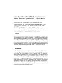
2 Each byte is preceded by one START bit and followed by one STOP bit in order to synchronize reception of the data, as shown in Figure 1. A typical MIDI message is composed of three bytes, and the second byte contains the note number; it can specify 128 different musical note numbers, spanning about 10 octaves. In this assignment, you are going to store and display only the 7 least significant bits of the second byte, that is, the note number, in binary. Figure 1. Timing of a MIDI byte 2. Project Description You are to design a serial port for the MIDI device that will read a MIDI signal, interpret its content and displays the note number (from the second byte) in binary on seven LEDs.
3 The MIDI signal will come from the PC via MIDI OX as in Lab 2. The notes played on the computer s keyboard will cause MIDI data to be sent serially out the MIDI OUT connector. This signal will be connected to a MIDI IN connector on your breadboard. The input stage of your circuit will include an optical isolator device, the 6N138 to ensure that there is no direct electrical link between the devices. This eliminates many problems associated with noise and ground loops. 3. Design Specification The MIDI standard specifies a uni-directional serial interface running at 31,250 bits/s 1%, a convenient division of the typical 4 MHz clock rate to be used in this lab.
4 Figure 2 illustrates the principle of decoding the MIDI message. It follows the general design of a USART or UART with the main exceptions being that the baud rate is fixed and it only operates in receive mode. A START bit and a STOP bit frame each byte. For transmission at 31,250 bits/s, each bit persists on the line for 32 s, called the bit time (BT). The addition of the start bit and stop bits means that each byte of the MIDI bytes takes 10 bit periods to transmit. However, the consecutive 10-bit frames may be separated by no time at all or an idle time of an undefined duration. Your design must not make the assumption that a stop bit is followed directly by a start bit.
5 You should verify this in simulation. Before the first frame is transmitted, the signal line idles high (1). The receiver monitors the line, waiting for the signal to drop to 0. Once the negative-going transition is detected, the receiver synchronizes on this transition and starts sampling the incoming serial stream. Conceptually, the receiver reads the 8 bits of the serial data by sampling the input in the middle of each bit, , at BT (bit0), BT (bit1), .., BT (bit7), as shown in Figure 1. Finally, the STOP bit could be sampled at BT, and the procedure is repeated for the next byte, synchronizing on the start bit. There are several methods that can be used for such a sampling.
6 Typically microcontroller UART modules sample the data at a rate 16x or 8x of the transmitted message. If the sampling at BT of the STOP bit does not produce the expected high value, the receiver sets a flag to indicate a framing error. Furthermore, several samples are made for each bit and the system uses voting to make sure that consistent data and the right bits are detected. In this experiment you are allowed to sample each bit once, provided that you use the correct sampling frequency. You are not required to implement any framing error detection. 4. Implementation In this experiment you will design a hardware version of a serial MIDI receiver. You ll find the schematic in the slides on the course site.
7 The design is to be implemented in Altera s Complex Programmable Logic Device (CPLD) MAX 7000S. Specifically, you will use a device from the MAX 7000S family with part number EPM7064 SLC44-10. Input to the Altera device is a single-bit input line from the MIDI interface cable through the opto-isolator circuit. The Altera chip will be clocked by a 4 MHz crystal oscillator, from which you may have to derive local clock for sampling (or, alternatively, count the faster clock to make sure you sample in the middle of each bit). Output of the device will drive seven LEDs to display the note number of the note played on computer keyboard in binary.
8 Note: Since two consecutive 10-bit frames may be separated by an unknown amount of idle time, you must devise a synchronization scheme whereby a START bit is detected for each byte of the three bytes messages separately. You cannot rely on synchronization of the START bit of the first byte only. Furthermore, since the MIDI signal is transmitted asynchronously, sampling it by the receiving synchronous device may violate the setup or hold time of the input flip-flop, which may result in metastability. A simple approach to avoid metastability in ICs is to add an additional flip-flop in the design to synchronize the incoming asynchronous signal with the new clock domain, as shown in lecture slides.
9 You will use Altera s Quartus II software to design, simulate, synthesize and program your design on a CPLD MAX 7000S programmable logic device. The student version of the software is provided in your kits. You will use verilog as the hardware description language for your design, and will simulate it using Quartus II waveform simulator. A short tutorial on how to use Quartus is available in the lecture slides and video on the class website; a complete tutorial is available in the Help menu of the Quartus II software. We will give a lecture on verilog , and there are numerous examples of verilog code available online. You should plan out the modules of your design and their connections before you start writing verilog code.
10 Note that multiple modules are required for full credit, so think about how you might decompose your design. Be sure to include only assignments (and not combinational logic) in your sequential blocks, following the style indicated in the verilog lecture slides. It is important that you simulate your design thoroughly before programming the chip and wiring up the board. After simulating the design, you will program it using Altera s USB-based JTAG programmer provided in your lab kit. You will also use a logic analyzer to thoroughly analyze the design when running on the breadboard. The simulation traces and logic analyzer traces will be an essential part of the project report.