Transcription of N-Channel Enhancement Mode MOSFET - Sync …
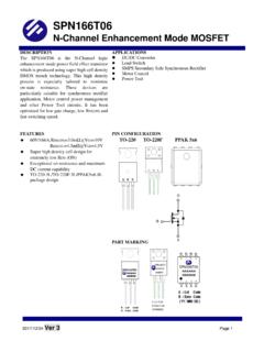
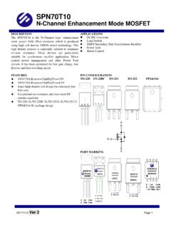
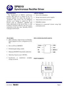
1 2008/05/05 Page 1 SPN2302 N-Channel Enhancement Mode MOSFET DESCRIPTION APPLICATIONS The SPN2302 is the N-Channel logic Enhancement mode power field effect transistors are produced using high cell density , DMOS trench technology. This high density process is especially tailored to minimize on-state resistance. These devices are particularly suited for low voltage application such as cellular phone and notebook computer power management and other battery powered circuits, and low in-line power loss are needed in a very small outline surface mount package.
2 Z Power Management in Note book z Portable Equipment z Battery Powered System z DC/DC Converter z Load Switch z DSC z LCD Display inverter FEATURES PIN CONFIGURATION(SOT-23-3L) PART M AR KIN G 20 ,RDS(ON)= 80m 20 ,RDS(ON)= 95m Super high density cell design for extremely low RDS (ON) Exceptional on-resistance and maximum DC current capability SOT-23-3L package design 2008/05/05 Page 2 SPN2302 N-Channel Enhancement Mode MOSFET PIN DESCRIPTION Pin Symbol Description 1 G Gate 2
3 S Source 3 D Drain ORDERING INFORMATION Part Number Package Part Marking SPN2302S23RG SOT-23-3L 02YW SPN2302S23 RGB SOT-23-3L 02YW Week Code : A ~ Z( 1 ~ 26 ) ; a ~ z( 27 ~ 52 ) SPN2302S23RG : Tape Reel ; Pb Free SPN2302S23RG : Tape Reel ; Pb Free.
4 Halogen Free ABSOULTE MAXIMUM RATINGS (TA=25 Unless otherwise C noted) Parameter Symbol Typical Unit Drain-Source Voltage VDSS 20 V Gate Source Voltage VGSS 12 V TA=25 C Continuous Drain Current(TJ=150) C TA=70 C ID A Pulsed Drain Current IDM 10 A Continuous Source Current(Diode Conduction)
5 IS A TA=25 C Power Dissipation TA=70 C PD W Operating Junction Temperature TJ 150 C Storage Temperature Range TSTG -55/150 C Thermal Resistance-Junction to Ambient R JA 100 /W C 2008/05/05 Page 3 SPN2302 N-Channel Enhancement Mode MOSFET ELECTRICAL CHARACTERISTICS (TA=25 Unless otherwise noted) C Parameter SymbolConditions Min.
6 Typ Drain-Source Breakdown Voltage V(BR)DSSVGS=0V,ID=250uA 20 Gate Threshold Voltage VGS(th)VDS=VGS,ID=250uA V Gate Leakage Current IGSS VDS=0V,VGS= 12V 100 nAVDS=20V,VGS=0V 1 Zero Gate Voltage Drain Current IDSS VDS=20V,VGS=0V TJ=55 C 10 uAVDS 5V,VGS= 6 On-State Drain Current ID(on)
7 VDS 5V,VGS= 4 A VGS= ,ID= On-Resistance RDS(on)VGS= ,ID= Forward Transconductance gfs VDS=5V,ID= 10 S Diode Forward Voltage VSD IS= ,VGS=0V V Dynamic Total Gate Charge Qg 10 Gate-Source Charge Qgs Gate-Drain Charge Qgd VDS=10V.
8 VGS= ID nCInput Capacitance Ciss 340 Output Capacitance Coss 115 Reverse Transfer Capacitance Crss VDS=10V,VGS=0V f=1 MHz 33 pFtd(on) 12 25 Turn-On Time tr 36 60 td(off)
9 34 60 Turn-Off Time tf VDD=10V,RL= ID ,VGEN= RG=6 10 25 ns 2008/05/05 Page 4 SPN2302 N-Channel Enhancement Mode MOSFET TYPICAL CHARACTERISTICS 2008/05/05 Page 5 SPN2302 N-Channel Enhancement Mode MOSFET TYPICAL CHARACTERISTICS 2008/05/05 Page 6 SPN2302 N-Channel Enhancement Mode MOSFET TYPICAL CHARACTERISTICS 2008/05/05
10 Page 7 SPN2302 N-Channel Enhancement Mode MOSFET SOT-23-3L PACKAGE OUTLINE 2008/05/05 Page 8 SPN2302 N-Channel Enhancement Mode MOSFET Information provided is alleged to be exact and consistent. SYNC Power Corporation presumes no responsibility for the penalties of use of such information or for any violation of patents or other rights of third parties which may result from its use. No license is granted by allegation or otherwise under any patent or patent rights of SYNC Power Corporation.