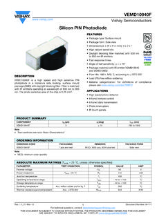
Transcription of Silicon PIN Photodiode - Vishay
1 VEMD5060X01. Vishay Semiconductors Silicon PIN Photodiode FEATURES. Package type: surface mount Package form: top view Dimensions (L x W x H in mm): 5 x 4 x Radiant sensitive area (in mm2): AEC-Q101 qualified High photo sensitivity High radiant sensitivity Excellent Ira linearity Suitable for visible and near infrared radiation DESCRIPTION Fast response times VEMD5060X01 is a high speed and high sensitive PIN Angle of half sensitivity: = 65 . Photodiode with a highly linear photoresponse. It is a low Floor life: 72 h, MSL 4, according to J-STD-020. profile surface mount device (SMD) including the chip with a Material categorization: for definitions of compliance mm2 sensitive area detecting visible and near infrared please see radiation.
2 APPLICATIONS. High speed photo detector Small signal detection Proximity sensors PRODUCT SUMMARY. COMPONENT Ira ( A) (deg) (nm). VEMD5060X01 26 65 350 to 1070. Note Test conditions see table Basic Characteristics . ORDERING INFORMATION. ORDERING CODE PACKAGING REMARKS PACKAGE FORM. VEMD5060X01 Tape and reel MOQ: 1000 pcs, 1000 pcs/reel Top view VEMD5060X01-GS15 Tape and reel MOQ: 5000 pcs, 5000 pcs/reel Top view Note MOQ: minimum order quantity ABSOLUTE MAXIMUM RATINGS (Tamb = 25 C, unless otherwise specified). PARAMETER TEST CONDITION SYMBOL VALUE UNIT. Reverse voltage VR 20 V. Power dissipation Tamb 25 C PV 240 mW.
3 Junction temperature Tj 110 C. Operating temperature range Tamb -40 to +110 C. Storage temperature range Tstg -40 to +110 C. Soldering temperature According to reflow solder profile fig. 8 Tsd 260 C. Thermal resistance junction / ambient According to EIA / JESD51 RthJA 350 K/W. ESD safety HBM 2000 V, k , 100 pF, 3 pulses ESDHBM 2 kV. Rev. , 21-Mar-16 1 Document Number: 84278. For technical questions, contact: THIS DOCUMENT IS SUBJECT TO CHANGE WITHOUT NOTICE. THE PRODUCTS DESCRIBED HEREIN AND THIS DOCUMENT. ARE SUBJECT TO SPECIFIC DISCLAIMERS, SET FORTH AT VEMD5060X01. Vishay Semiconductors BASIC CHARACTERISTICS (Tamb = 25 C, unless otherwise specified).
4 PARAMETER TEST CONDITION SYMBOL MIN. TYP. MAX. UNIT. Forward voltage IF = 50 mA VF - V. Breakdown voltage IR = 100 A, E = 0 V(BR) 20 - - V. Reverse dark current VR = 10 V, E = 0 Iro - 10 nA. VR = 0 V, f = 1 MHz, E = 0 CD - 80 - pF. Diode capacitance VR = 3 V, f = 1 MHz, E = 0 CD - 35 40 pF. Open circuit voltage Ee = 1 mW/cm2, = 950 nm Vo - 350 - mV. Temperature coefficient of Vo Ee = 1 mW/cm2, = 950 nm TKVo - - mV/K. Short circuit current Ee = 1 mW/cm2, = 950 nm Ik - 26 - A. Temperature coefficient of Ik Ee = 1 mW/cm2, = 835 nm TKIk - - %/K. Ee = 1 mW/cm2, = 950 nm, VR = 5 V Ira 20 26 31 A. Reverse light current Ee = 1 mW/cm2, = 890 nm, VR = 5 V Ira - 38 - A.
5 Angle of half sensitivity - 65 - deg Wavelength of peak sensitivity p - 820 - nm Range of spectral bandwidth - 350 to 1070 - nm Rise time VR = 5 V, RL = 50 , = 820 nm tr - 30 - ns Fall time VR = 5 V, RL = 50 , = 820 nm tf - 30 - ns BASIC CHARACTERISTICS (Tamb = 25 C, unless otherwise specified). Basic characteristics graphs to be extended to 110 C ambient temperatures where applicable. 1000 VR = 10 V 940 nm Iro - Reverse Dark Current (nA). Ira rel - Relative Reverse Light Current VR = 10 V. 100. 865 nm 10. 1 835 nm -40 -20 0 20 40 60 80 100 -40 -20 0 20 40 60 80 100. Tamb - Ambient Temperature ( C) Tamb - Ambient Temperature ( C).
6 Fig. 1 - Reverse Dark Current vs. Ambient Temperature Fig. 2 - Relative Reverse Light Current vs. Ambient Temperature Rev. , 21-Mar-16 2 Document Number: 84278. For technical questions, contact: THIS DOCUMENT IS SUBJECT TO CHANGE WITHOUT NOTICE. THE PRODUCTS DESCRIBED HEREIN AND THIS DOCUMENT. ARE SUBJECT TO SPECIFIC DISCLAIMERS, SET FORTH AT VEMD5060X01. Vishay Semiconductors S( )rel - Relative Spectral Sensitivity 1000. VR = 5 V, = 950 nm Ira - Reverse Light Current ( A). 100 10. 1. 0. 1 10 400 500 600 700 800 900 1000 1100. Ee - Irradiance (mW/cm2) - Wavelength (nm). Fig. 3 - Reverse Light Current vs. Irradiance Fig.
7 6 - Relative Spectral Sensitivity vs. Wavelength 1000. = 950 nm 0 10 20 . Ira - Reverse Light Current ( A). 10 mW/cm2 30 . mW/cm2 Srel - Relative Radiant Sensitivity 100. - Angular Displacement mW/cm2. mW/cm2. mW/cm2. 40 . 10 mW/cm2. mW/cm2 50 . mW/cm2. 1 60 . mW/cm2. mW/cm2. 70 . 80 . 1 10 100. VR - Reverse Voltage (V) 0. Fig. 4 - Reverse Light Current vs. Reverse Voltage Fig. 7 - Relative Radiant Sensitivity vs. Angular Displacement 90. 80 f = 1 MHz, E = 0. 70. CD - Capacitance (pF). 60. 50. 40. 30. 20. 10. 0. 1 10 100. VR - Reverse Voltage (V). Fig. 5 - Diode Capacitance vs. Reverse Voltage Rev. , 21-Mar-16 3 Document Number: 84278.
8 For technical questions, contact: THIS DOCUMENT IS SUBJECT TO CHANGE WITHOUT NOTICE. THE PRODUCTS DESCRIBED HEREIN AND THIS DOCUMENT. ARE SUBJECT TO SPECIFIC DISCLAIMERS, SET FORTH AT VEMD5060X01. Vishay Semiconductors PACKAGE DIMENSIONS in millimeters 4. Bottom view 5. 3. Optical window Optical 3. center Top view C (20 : 1). C Tie bar, electrically connected to cathode 2. Recommended footprint Cathode 1. Exposed pad 1. (cathode). Center of device (4 x). 1. NC. 2 Anode (4 x). Technical drawings Not indicated tolerances according to DIN. Drawing- No.: specification Issue: 2; Rev. , 21-Mar-16 4 Document Number: 84278.
9 For technical questions, contact: THIS DOCUMENT IS SUBJECT TO CHANGE WITHOUT NOTICE. THE PRODUCTS DESCRIBED HEREIN AND THIS DOCUMENT. ARE SUBJECT TO SPECIFIC DISCLAIMERS, SET FORTH AT VEMD5060X01. Vishay Semiconductors TAPE AND REEL DIMENSIONS in millimeters Reel-design is reperesentative for different types Unreel direction X. Label posted here B-B ( 2 : 1 ). B. X. 2. 8. Anode B Drawing-No.: ;. Issue: 1; Rev. , 21-Mar-16 5 Document Number: 84278. For technical questions, contact: THIS DOCUMENT IS SUBJECT TO CHANGE WITHOUT NOTICE. THE PRODUCTS DESCRIBED HEREIN AND THIS DOCUMENT. ARE SUBJECT TO SPECIFIC DISCLAIMERS, SET FORTH AT VEMD5060X01.
10 Vishay Semiconductors SOLDER PROFILE DRYPACK. Devices are packed in moisture barrier bags (MBB) to 300 prevent the products from moisture absorption during max. 260 C transportation and storage. Each bag contains a desiccant. 250 255 C. 240 C 245 C. 217 C. FLOOR LIFE. Temperature ( C). 200 Time between soldering and removing from MBB must not max. 30 s exceed the time indicated in J-STD-020: 150. Moisture sensitivity: level 4. max. 120 s max. 100 s 100. Floor life: 72 h max. ramp down 6 C/s Conditions: Tamb < 30 C, RH < 60 %. 50 max. ramp up 3 C/s DRYING. 0 In case of moisture absorption devices should be 0 50 100 150 200 250 300.