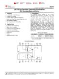
Transcription of Linearization using Analog Pre Distortion - IEEE ComSoc SCV
1 Linearization using Analog Pre Distortion RAJEEV KRISHNAMOORTHY. PRESENTATION AT IEEE ComSoc . FEBRUARY 8, 2012. Semiconductors for Wireless Communications Scintera Confidential Provided under NDA 1. Scintera Overview Technology Programmable Analog signal processing platform delivering higher performance and f d lower power consumption versus traditional DSP solutions l i di i l DSP l i the programmability of digital but the simplicity, size and power of Analog Standard CMOS process Initial Products: RF Power Amplifier Linearizer (RFPAL). Single Chip power amplifier Linearization Changing the paradigm for PA Linearization making it simple, small and cost effective across a broad range of applications ISO9001 Certified Semiconductors for Wireless Communications Scintera Confidential Provided under NDA. Product Highlights Fi t RF PA Li i (RFPAL) i f ll d ti SC1887 First RF PA Linearizer (RFPAL) in full production Sampled in August 2009 & released to production in February 2010.
2 > 20 customers in production with > 35 designs 2G/3G Cellular Infrastructure Broadcast Microwave Backhaul 100k+ operating reliably in the field SC1889 & SC1869 2nd generation RFPAL in full production Optimized for LTE, TD LTE. Optimized for LTE, TD and WiMax + 3G. LTE and WiMax + 3G. Launch LTE customers now in production further ramps throughout 2012. Extended function to precision RMS power measurement Sweet spot in small cell applications SC1894 extending functionality and performance, sampling in Q2 2012. Semiconductors for Wireless Communications Scintera Confidential Provided under NDA. PA Linearization Overview Semiconductors for Wireless Communications Scintera Confidential Provided under NDA. PA Linearization Techniques Power Added Efficiency, including power supply regulations (%) vs year of introduction for PA output power ~50. vs. year of introduction for PA output power 50 W & 5W.
3 W & 5W. Semiconductors for Wireless Communications Scintera Confidential Provided under NDA 5. Digital Pre Distortion (DPD). Benefits Programmable, customizable for particular application, control Challenges High power consumption, high frequency reconstruction filter, wide band up-mixer, challenging clock generation to achieve converters SNR, lack of modularity, cost . Semiconductors for Wireless Communications Scintera Confidential Provided under NDA 6. RFPAL (RF PA Linearization ). Benefits: Lower power digital processor, easy reconstruction filter, relaxed up mixer requirements, low power, low cost, easy to use; modular; feedback path fully integrated; DAC deals with 1x signal bandwidth Challenges Potentially degree of control for end user Semiconductors for Wireless Communications Scintera Confidential Provided under NDA 7. RFPAL System Architecture & RFPAL S t A hit t &.
4 Implementation p Semiconductors for Wireless Communications Scintera Confidential Provided under NDA. RFPAL Application Semiconductors for Wireless Communications Scintera Confidential Provided under NDA 9. RFPAL System Architecture RF SSIGNAL PROCESSOR. RFIN RFOUT. Envelope Analog . Correction Processor Correction Processor DIGITAL LOGIC P. Initialize EEPROM. Down Convert Generate Spectrum Calibrate & CLK. Power Analysis Adapt & Track Sample RFFB Generate Corr. Func. SPI. Semiconductors for Wireless Communications Scintera Confidential Provided under NDA 10. Cost Function PIE. Optimize C ( w ) log 2 f1 P1L , P1U f 2 ( P2 L , P2U ) f 3 PIE . Cost function Cost function w opt min C ( w ). w Use a Stochastic gradient search algorithm to optimize g g p Semiconductors for Wireless Communications Scintera Confidential Provided under NDA 11. Adaptation & Tracking Small Steps / Slow Conv.
5 P 8 LSB P 1 LSB. = 1/2. 1/2 P 4 LSB. 4 LSB = 1/16. 1/16. = 1/8. Large Steps / Steady State / Fast Conv. Track Semiconductors for Wireless Communications Scintera Confidential Provided under NDA 12. RFPAL Signal Path Moves signal processing application from digital to Analog domain Semiconductors for Wireless Communications Scintera Confidential Provided under NDA 13. Analog Volterra Series 4 5. VIN(t) r (t). 2 VOUT(t) ~ (t - p ). c r p 1 m 1. Semiconductors for Wireless Communications Scintera Confidential Provided under NDA 14. Linearizing Time Slotted & 4G Waveforms Semiconductors for Wireless Communications Scintera Confidential Provided under NDA. LTE05MD56# -1. LTE 05M D56# at, duty fac tor = dB , P A R = dB. 10. -2. 10. CCDF. -3. 10. -4. 10 k urtos is = 4 5 6 7 8 9 10 11 12. P eak -to-average power ratio, dB. L T E 0 5 M D 5 6 # 1 1 . 0 4 . m a t , d w e l l = 2 0 s , d u t y fa c t o r = - 2.
6 5 4 d B LTE 05M D56# at, duty fac tor = dB , -30 dB c B W = M Hz 20. p e a k a c ro s s 2 0 u s 12 kHz LP F 10. 0. 0. -10. Signal amplitude, dBFS. -5. -20 A verage M ax Hold PSD, dB. -30. -1 0. -40. 40. -50. -1 5 -60. -70. -2 0 -80. 0 1 2 3 4 5 6 7 8 9 10 -3 -2 -1 0 1 2 3. T im e , m s F requenc y , M Hz Semiconductors for Wireless Communications Scintera Confidential Provided under NDA 16. Problem: Poor Performance with Power Perturbation Semiconductors for Wireless Communications Scintera Confidential Provided under NDA 17. Range of Compensation PA Transfer Function Full Power/All Carriers Full Power/All Carriers Backed Off / Some Carriers Expanded Range of Correction Expanded Range of Correction Semiconductors for Wireless Communications Scintera Confidential Provided under NDA 18. Some Results Semiconductors for Wireless Communications Scintera Confidential Provided under NDA.
7 Macro: 30W LTE 20 MHz , p , drain= 39%. PAR = dB, Amplifier P3dB = dBm, . SN460 PAM121 25 LTE20M1%100# MHz 11/01/24 11:01:27 U BO= SN460 PAM121 25 LTE20M1%100# MHz 11/01/24 11:01:27 U. -25 20. POUT-0 = dBm PSD-1. WP. ACLR1-0 POUT-1 = dBm PSD-0. -30 10. ACLR1-1 ACLR2L-0 ACLR1L-0 ACLR1U-0 ACLR2U-0. ACLR2 0. ACLR2-0 49 7 31 6 31 0 50 6. ut Power, dBm / 30 kHz -35. ACLR2-1 0 ACLR2L-1 ACLR1L-1 ACLR1U-1 ACLR2U-1. -40. ACLR, dBc -10. -45. -20. -50. 50. PA Outpu -30. -55. -60 -40. -65 -50. 32 34 36 38 40 42 44 46 48 -50. 50 -40. 40 -30. 30 -20. 20 -10. 10 0 10 20 30 40 50. Pout, dBm Frequency Offset from Carrier Center, MHz Semiconductors for Wireless Communications Scintera Confidential Provided under NDA. LTE with Low Traffic Loading SC1889 performance with changing output power and variable frequency use SC1889 performance with changing output power and variable frequency use E-TM LTE20M1-1# , dwell = 20 s, duty factor = dB.
8 Peak across 20 us 0 12 kHz LPF. e, dBFS. -5. ue amplitude Amplitidu -10. Signal -15. 15. -20. 0 1 2 3 4 5 6 7 8 9 10. Time, ms Blue Uncorrected Yellow 100% Loaded Magenta Partial Loaded Signal Shown at Right Semiconductors for Wireless Communications Scintera Confidential Provided under NDA. RFPAL Key Architectural Attributes Analog Digital and SW partitioning minimize power & area Analog , Digital, and SW partitioning minimize power & area Computation of correction terms in digital (software and hardware) domain Application of correction in the Analog domain Flexible Work Function Synthesizes wide range of AM/AM and AM/PM & memory compensation (1ns . 300ns) Enables robust adaptation orthogonal basis terms of work function Enables robust adaptation orthogonal basis terms of work function Robust performance with process, voltage, aging and temperature variations Extensive digital/ Analog compensation loops for Analog cells, with process/temp Extensive digital/ Analog compensation loops for Analog cells, with process/temp sensing, calibration routines Optimized calibration algorithms using a low power, on chip spectral estimator.
9 Software driven Analog circuit design that can be conveniently tuned /optimized. Software driven correction enables flexibility With respect to waveforms, PA, power consumption, duty cycle, etc. Allows customization of solutions by application and customer Allows customization of solutions by application and customer Semiconductors for Wireless Communications Scintera Confidential Provided under NDA 22. Q & A. Semiconductors for Wireless Communications Scintera Confidential Provided under NDA 23.