Search results with tag "Transconductance"

LM13600 Dual Operational Transconductance Amplifiers with ...
www.sdiy.orgTL/H/7980 LM13600 Dual Operational Transconductance Amplifiers with Linearizing Diodes and Buffers February 1995 LM13600 Dual Operational Transconductance

ZVP2106A P-channel enhancement mode vertical DMOS FET ...
www.diodes.comTransconductance v drain current ID- Drain Current (Amps) g fs-T ra n sc o ndu c t a ductance (mS) 0 Q-Charge (nC) Transconductance v gate-source voltage VGS-Gate Source Voltage (Volts) f s-T rans c n 0-10 -20 -30 VDS-Drain Source Voltage (Volts) Capacitance v drain-source voltage C-Capacitance (pF) Coss V G S-Gate Sou r ce V oltag e (V o lts ...
The Art of Electronics
artofelectronics.net2.2.9 Transconductance 89 2.3 Ebers–Moll model applied to basic tran-sistor circuits 90 2.3.1 Improved transistor model: transconductance amplifier 90 2.3.2 Consequences of the Ebers–Moll model: rules of thumb for transistor design 91 2.3.3 The emitter follower revisited 93 2.3.4 The common-emitter amplifier revisited 93
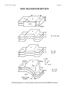
MOS TRANSISTOR REVIEW - Stanford University
web.stanford.edu3. Improve current drive (transconductance gm) g I V V const W L K t V V linear region W L K t V V V saturation region m D G D n ox ox DD n ox ox GT D SAT SAT = = ≈< ≈−()> ∂ ∂ µ µ for V for V D D,, Decreasing the channel length and gate oxide thickness increases gm, i.e., the current drive of the transistor. Much of the scaling is ...
SNOSBW2F –NOVEMBER 1999–REVISED NOVEMBER 2015 …
www.ti.comProduct Folder Sample & Buy Technical Documents Tools & Software Support & Community LM13700 SNOSBW2F –NOVEMBER 1999–REVISED NOVEMBER 2015 LM13700 Dual Operational Transconductance Amplifiers

Wide Bandwidth Operational Transconductance Amplifier …
www.ti.comOPA861 www.ti.com SBOS338G – AUGUST 2005– REVISED MAY 2013 ELECTRICAL CHARACTERISTICS: VS = ±5V RL = 500Ωand RADJ = 250Ω, unless otherwise noted. OPA861ID, IDBV TYP MIN/MAX OVER TEMPERATURE 0°C to – 40°C to MIN/ TEST

TUTORIAL CADENCE DESIGN ENVIRONMENT
web.itu.edu.trCadence tools. A simple Operational Transconductance Amplifier (OTA) will be designed in the AMI 0.5µm CMOS technology. However, the same procedures apply to complete chip designs. 5.1. Library creation and selection of technology It is recommended that you use a library to store related cell views; e.g., use a library to hold all the

(Saturated) MOSFET Small-Signal Model Transconductance
inst.eecs.berkeley.eduEE 105 Fall 1998 Lecture 11 p-channel MOSFET small-signal model the source is the highest potential and is located at the top of the schematic gmvsg gmbvsb ro gate drain bulk + _ vsg Cgs C sb Cdb Cgd gb _ source −id vsb

ZVN3310A N-channel enhancement mode vertical DMOS FET ...
www.diodes.comTransconductance v drain current ID- Drain Current (Amps) g f s-T ransconductance (mS) g f s-T rans c o n ducta n ce (m S) 0 80 0 40 120 160 VDS= 25V 0.2 0.4 0.6 0.8 1.0 1.2 0 80 0 40 120 160 VDS= 25V 24 6 8 10 12 VDS-Drain Source Voltage (Volts) Capacitance v drain-source voltage C-p a c ita nce (pF) Coss Ciss Crss 0 10 20 30 40 50 0 30 20 10 ...

MT-079: Analog Multipliers - Analog Devices
www.analog.comFigure 4: Basic Transconductance Multiplier . This is a rather poor multiplier because (1) the Y input is offset by the VBE which changes non-linearly with VY; (2) the X input is non-linear as a result of the exponential relationship between IC and VBE; and (3) the scale factor varies with temperature. Page 3 of 8

Measuring Power MOSFET Characteristics
www.vishay.comThis is the forward transconductance of the device at a specified value of ID. gfs represents the signal gain (drain current divided by gate voltage) in the linear region. This parameter should be measured with a small AC superimposed on a gate bias an d the curve tracer is not the appropriate tool for this measurement. Even with specific

LM324 - Single Supply Quad Operational Amplifiers
www.onsemi.comThe transconductance reduction is accomplished by splitting the collectors of Q20 and Q18. Another feature of this input stage is that the input common mode range can include the negative supply or ground, in single supply operation, without saturating either the input

Lecture 17: Common Source/Gate/Drain Amplifiers
inst.eecs.berkeley.eduGeneric Transconductance Amp. Department of EECS University of California, Berkeley EECS 105Fall 2003, Lecture 17 Prof. A. Niknejad Two-Port CS Model Reattach source and load one-ports: Department of EECS University of California, Berkeley EECS 105Fall 2003, Lecture 17 Prof. A. …

C2M0040120D C2M SiC MOSFET
assets.wolfspeed.comfs Transconductance 18.2 S V DS= 20 V, I DS= 40 A Fig. 7 17.2 V DS= 20 V, I DS= 40 A, T J = 150 °C C iss Input Capacitance 2440 pF V GS = 0 V V DS = 1000 V f = 1 MHz V AC = 25 mV Fig. 17,18 C oss Output Capacitance 171 C rss Reverse Transfer Capacitance 11 E oss C oss Stored Energy 89 μJ Fig 16 E ON Turn-On Switching Energy (Body Diode) 1.7 ...

IRF520 9.2A, 100V, 0.270 Ohm, N-Channel Power MOSFET
www.pcbheaven.comForward Transconductance (Note 2) gfs V DS ≥ 50V, I D = 5.6A (Figure 12) 2.7 4.1 - S Turn-On Delay Time t d(ON) V DD = 50V, I D ≈ 9.2A, R G = 18 Ω, R L = 5.5 Ω MOSFET Switching Times are Essentially Independent of Operating Temperature - 9 13 ns Rise Time t r-30 63 ns Turn-Off Delay Time t d(OFF)-18 70 ns Fall Time t f-20 59 ns Total Gate ...

Engineering Science Data Booklet Higher - SQA
www.sqa.org.ukTypical operational amplifier circuits ..... 8—10 Preface This data booklet is intended for use by candidates in examinations in Engineering Science at ... MOSFET transconductance g m = ∆I d/∆V gs. Page eight Typical operational amplifier circuits ( ) R f = feedback resistance R i = input resistance Inverting Non-inverting output voltage ...
Demystifying the Operational Transconductance Amplifier ...
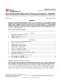
www.ti.com3 B 2 E C 8 V I OPA861 100 W R E R L V O Noninverting Gain V = 0VOS Transconductor (used here) C B E Diamond Transistor 3 2 1 V IN2 IOUT V IN1 Voltage-Controlled Current Source IOUT V IN2 V IN1 Z CCII+ Current Conveyor II+
Transconductance - University of Arizona
atlas.physics.arizona.eduField effect transistors Similarly, in field effect transistors, and MOSFETs in particular, transconductance is the change in the drain current divided by the small change in the gate/source voltage with a constant drain/source voltage. Typical values of g m for a small-signal field effect transistor are 1 to 30 millisiemens.
Similar queries
LM13600 Dual Operational Transconductance Amplifiers, LM13600 Dual Operational Transconductance Amplifiers with Linearizing, Transconductance, The Art of Electronics, Operational Transconductance, Operational Transconductance Amplifier, Fall, Potential, T ransconductance, T rans c o n ducta n ce, Analog Devices, Operational, Field effect transistors, Field effect