Transcription of 3.3 V powered, 15 kV ESD protected, up to 12 Mbps RS-485 ...
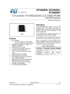
1 November 2007 Rev 51 V powered, 15 kv esd protected ,up to 12 Mbps RS-485 /RS-422 transceiverFeatures ESD protection 15 kV human body model 8 kV IEC 1000-4-2 contact discharge Operate from a single V supply - no charge pump required Interoperable with 5 V logic 1 A low current shutdown mode max Guaranteed 12 Mbps data rate -7 to 12 V common mode input voltage range Half duplex versions available Industry standard 75176 pinout Current limiting and thermal shutdown for driver overload protection Guaranteed high receiver output state for floating inputs with no signal present Allow up to 64
2 Transceivers on the busDescriptionThe ST3485E is 15 kv esd protected , V low power transceiver for RS-485 and RS-422 communications. The device contains one driver and one receiver in half duplex configuration. The ST3485E transmits and receives at a guaranteed data rate of at least 12 transmitter outputs and receiver inputs are protected to 15 kV using Human Body is short-circuit current limited and is protected against excessive power dissipation by thermal shutdown circuitry that places the driver outputs into a high-impedance SO-8 Table summaryOrder codeTemperature rangePackagePackagingST3485 ECN0 to 70 CDIP-850 parts per tube / 40 tube per boxST3485 ECDR0 to 70 CSO-8 (tape and reel)2500 parts per reelST3485 EBDR-40 to 85 CSO-8 (tape and reel)
3 2500 parts per - ST3485EC2/22 Contents1 Pin configuration .. 32 Truth tables .. 43 Maximum ratings .. 54 Electrical characteristics .. 65 Test circuits and typical characteristics .. 96 Package mechanical data .. 177 Revision history .. 21ST3485EB - ST3485 ECPin configuration3/22 1 Pin configuration Figure connectionsTable descriptionPin n SymbolName and function1 ROReceiver output. If A>B by 200mV, RO will be high; if A<B by 200mV, RO will be low2 REReceiver output enable. RO is enabled when RE is low; RO is high impedance when RE is high.
4 If RE is high and DE is low, the device will enter a low power shutdown output enable. The driver outputs are enabled by bringing DE high. They are high impedance when DE is low. If RE is high DE is low, the device will enter a low-power shutdown mode. If the driver outputs are enabled, the part functions as line driver, while they are high impedance, it functions as line receivers if RE is input. A low on DI forces output A low and output B high. Similarly, a high on DI forces output A high and output B low5 GNDG round6 ANon-inverting receiver input and non-inverting driver output7 BInverting receiver input and inverting driver output8 VCCS upply voltage: VCC= 3V to tablesST3485EB - ST3485EC4/22 2 Truth tables Note:X= Don t care; Z=High impedance Note:X= Don t care.
5 Z=High impedanceTable table (driver)InputsOutputsModeREDEDIBAXHHLHN ormalXHLHLN ormalLLXZZN ormalHLXZZS hutdownTable table (receiver)InputsOutputModeREDEA-BROLL OpenHNormalHLXZS hutdownST3485EB - ST3485 ECMaximum ratings5/22 3 Maximum ratingsNote:Absolute maximum ratings are those values beyond which damage to the device may occur. Functional operation under these condition is not implied. Table maximum ratingsSymbolParameterValueUnitVCCS upply voltage7 VVIC ontrol input voltage (RE, DE) to 7 VVDID river input voltage (DI) to 7 VVDOD river output voltage (A, B) 14 VVRIR eceiver input voltage (A, B) 14 VVROR eceiver output voltage (RO) to (VCC + )VTable performance.
6 Transmitter outputs, receiver inputsSymbolParameterTest protection voltageHuman body model 15kVESDESD protection voltageIEC-1000-4-2 Contact discharge 8kVElectrical characteristicsST3485EB - ST3485EC6/22 4 Electrical characteristics Table characteristics VCC = 3 V to V, TA = -40 to 85 C, unless otherwise specified. Typical values are referred to TA = 25 C)SymbolParameterTest Power supply current No Load, DI=0V or VCCDE=VCC,RE=0V or , RE= supply currentDE=0V, RE=VCC, DI=0V or VCC ATable input electrical characteristics VCC = 3 V to V, TA = -40 to 85 C, unless otherwise specified.
7 Typical values are referred to TA = 25 C)SymbolParameterTest logic threshold lowDE, DI, logic threshold highDE, DI, RE2 VIIN1 Logic input currentDE, DI, RE AIIN2 Input current (A, B)DE=0V, VCC= 0 or electrical characteristics VCC = 3 V to V, TA = -40 to 85 C, unless otherwise specified. Typical values are referred to TA = 25 C)SymbolParameterTest drive outputRL= 100 (RS-422) (Figure 1)2 VRL= 54 ( RS-485 ) (Figure 1) 60 ( RS-485 ) (Figure 2) VODC hange in magnitude of driver differential output voltage for complementary output states (Note: 1)RL= 54 or 100 (Figure 1) common mode output voltageRL= 54 or 100 (Figure 1)3V VOCC hange in magnitude of driver common mode output voltage (Note.
8 1)RL= 54 or 100 (Figure 1) short circuit output current 250mAST3485EB - ST3485 ECElectrical characteristics7/22 Table electrical characteristics VCC = 3 V to V, TA = -40 to 85 C, unless otherwise specified. Typical values are referred to TA = 25 C)SymbolParameterTest differential threshold voltageVCM = -7V to 12V, DE = VTHR eceiver input hysteresisVCM = 0V70 VVOHR eceiver output high voltageIOUT = -4mA, VID = 200mV(Figure 8 and Figure 9)2 VVOLR eceiver output low voltageIOUT = 4mA, VID = -200mV, (Figure 3) (high impedance) output current at receiverVCC = , VO = 0V to VCC 1 ARRINR eceiver input resistanceVCM = -7V to 12V24k IOSRR eceiver short-circuit currentVRO = 0V to VCC760mATable switching characteristics VCC = 3 V to V, TA = -40 to 85 C, unless otherwise specified.
9 Typical values are referred to TA = 25 C)SymbolParameterTest data rate1215 MbpstDDDifferential output delayRL= 60 , CL = 15pF, (Figure 4 and Figure 5)1830nstTDDifferential output transition timeRL= 60 , CL = 15pF, (Figure 4 and Figure 5)1220nstPLHtPHLP ropagation delay RL= 27 , CL = 15pF, (Figure 8 and Figure 9)1830nstPDS|tPLH - tPHL| Propagation delay skew (Note 2)RL= 27 , CL = 15pF, (Figure 8 and Figure 9)25nstPZLO utput enable timeRL= 110 , (Figure 10 and Figure 11)1935nstPZHO utput enable timeRL= 110 , (Figure 6 and Figure 7)3050nstPHZO utput disable timeRL= 110 , (Figure 6 and Figure 7)1935nstPLZO utput disable timeRL= 110 , (Figure 10 and Figure 11)3050nstSKEWD ifferential output delay skew13nstZH(SHDN)Driver enable from shutdown to output high3050nstZL(SHDN)Driver enable from shutdown to output low1935nsElectrical characteristicsST3485EB - ST3485EC8/22 Note:1 VOD and VOC are the changes in VOD and VOC, respectively, when the DI input changes state.
10 2 Measured on |tPLH(A)-tPHL(A)| and |tPLH(B)-tPHL(B)|3 The transceivers are put into shutdown by bring RE high and DE low. If the input are in state for less than 80 ns, the part are guaranteed not to enter shutdown. If the inputs are in this state for at least 300 ns, the parts are guaranteed to have entered switching characteristics VCC = 3 V to V, TA = -40 to 85 C, unless otherwise specified. Typical values are referred to TA = 25 C)SymbolParameterTest delayVID =0V to 3V, CL1 = 15pF(Figure 12 and Figure 13)3050nstRPDS|tPLH - tPHL| Propagation delay skewVID =0V to 3V, CL1 = 15pF(Figure 12 and Figure 13)13nstPZLO utput enable timeCRL = 15pF, (Figure 14 and Figure 18)1020nstPZHO utput enable timeCRL = 15pF, (Figure 14 and Figure 18)1020nstPHZO utput disable timeCRL = 15pF, (Figure 14 and Figure 18)1020nstPLZO utput disable timeCRL = 15pF, (Figure 14 and Figure 18)1020nstZH(SHDN)