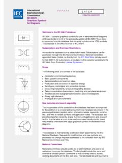
Transcription of IEC 61000-4-2 ESD S
1 Rev. 3/21 Copyright 2021 by Silicon LaboratoriesAN8951. IntroductionThis application note provides a brief overview about the possible ESD protecting realizations for any SiliconLabs RF designs. However, experimental measurements have only been taken with, and thus the efficiency ofthe ESD protection realizations has been demonstrated on, Si4x6x-based reference radio chips are designed for and tested against the different chip-level ESD standards such as Human BodyModel (HBM), Machine Model (MM) and Charged Device Model (CDM). These chip-level test results aresummarized in the RF IC s Qualification , in a real-world application the final module has to resist and stand against an ESD shock.
2 For thispurpose, the final electronic product has to be tested against a different, more stringent standard that simulatesand replicates the real world ESD stress conditions. This system-level standard is the IEC 61000 -4-2. System/module designers should take care to comply with the IEC 61000 -4-2 system-level ESD standard. Thisapplication note shows Silicon Labs customers how to achieve the best possible system-level protections onboard level using Silicon Labs radio Si4x6x Qualification ReportThe Si4x6x radios ESD robustness against the different chip level ESD standards are summarized in ElectricalVerification of the Qualification Report .The following is a brief summary from those results: ESD-HBM: pass up to 2 kV ESD-MM: pass up to 50 V for all pins, excluding RF pins if it is 200 V ESD-CDM: pass up to 500 V3.
3 Overview of IEC 61000 -4-2 StandardThe IEC standard is a system level test that replicates a charged person discharging to a system in a system enduser environment. The purpose of the system level test is to ensure that finished products can survive normaloperation and it is generally assumed that the user of the product will not take any ESD precautions to lower ESDstress to the product. The IEC 61000 -4-2 standard defines four standard levels of ESD protection, using two different testingmethodologies. Contact discharge involves discharging an ESD pulse directly from the ESD test gun that istouching the device under test. This is the preferred method of testing.
4 However, the standard provides for analternate test methodology known as air discharge for cases where contact discharge testing is not possible. Inthe air discharge test, the ESD test gun is brought close to the device under test until a discharge occurs. Thestandards are defined so that each level is considered equivalent a Level 4 contact discharge of 8 kV isconsidered equivalent to a 15 kV air discharge. IEC 61000 -4-2 ESD SYSTEM LEVEL PROTECTION AN895AN8952 Rev. Recommended ESD Test BenchFigure 1. IEC 61000 -4-2 Test Simulation CircuitThe IEC standard replicates a charged person discharging into a system in an uncontrolled environment. This testis performed to ensure the system will remain operational in an end user environment where no ESD stressprecautions are taken.
5 Figure 2. Simulation Circuit of IEC 61000 -4-2AN895 Rev. IEC 61000 -4-2 Test Pulse WaveformFigure 3. IEC 61000 -4-2 ESD Pulse WaveformContact DischargeAir DischargeLevelTest Voltage (kV)LevelTest Voltage (kV)12122424363848415AN8954 Rev. Peak Current of IEC 61000 -4-2 ESD StandardApplied Voltage (kV)Peak Current (A) 4. ESD Protection Circuit ExampleThis section contains an example of an ESD protection circuit that can effectively suppress an IEC 61000 -4-2 ESDshock. The following passive components can be included in an effective external ESD protection circuit: series resistors,ferrites, filtering capacitors and inductors, transient voltage suppressors ( , TVS diodes), thyristors, varistors,polymer, ESD protection circuit composed from these above components can block ESD currents and clamp ESD-induced high voltages.
6 The exceeded ESD currents can be suppressed and shunted to minimize the effects of theESD pulses in the system. It is highly recommended to place the protection circuit as close as possible to theconnection point on the board where the ESD shock event can occur. This placing approach can minimize thepossibility of causing further couplings of the ESD currents and voltages to the other blocks on the module. A general I/O connector of a piece of electrical equipment can be protected with the example circuit composed withexternal passive components shown in Figure 4. Example for ESD Protection CircuitJ1: connection point where the ESD shock occurs (high-voltage IEC 61000 -4-2 Test Pulse)J2: ESD-protected connection point (suppressed test signal)L1: series filtering inductorC1, C2: parallel filtering capacitorsD1: TVS diodeR: series resistorThe ESD shock is supposed to occur at the J1 point.
7 The L-C low-pass filtering section suppresses the fast ESDshock signal; the L1 inductor can block the large currents, while the C1 and C2 capacitors can limit the highvoltage induced by the transient fast current spike. The D1 TVS diode can be effectively used for suppressing the fast ramped-up ESD signals and plenty of thesekinds of diodes are available on the market from different manufacturers (specified for assisting equipment to passIEC 61000 -4-2, even level 4 testing). The optimum values for the components and even the optimum structure ( , it might not be necessary to use allof the shown components in Figure 4) depend on the level of the ESD signal, board layout, and on the terminationat the J2 point.
8 It is possible to select the filtering element values in a way where the largest suppression can be achieved at theGHz region, since the ramp-up time of the fast ESD signal is around 1 ns, as shown in Figure 3. AN8956 Rev. 5. Waveform Measurements as IEC 61000 -4-2 StandardSilicon Labs performed waveform measurements with the following setup: IEC 61000 -4-2 ESD standard test bench setup IEC 61000 -4-2 ESD standard test signals Direct contact waveform measurements from the IEC 61000 -4-2 test signal Contact waveform measurements with applying an example ESD protection circuitThis section illustrates how the waveforms look before (direct measurement of IEC 61000 -4-2 test signal) and afteran example ESD protection circuit.
9 In addition, this section demonstrates the effectiveness of the protection TVS diode used in the example protection circuit ( D1 ) is: ESD protection circuit was realized on a small PCB that only included the elements shown in Figure following figures show the measured waveforms with different conditions such as voltage of the test signal,different elements mounted on the ESD protection board, different element values, and etc. The conditions areidentified in each figure 5. IEC 61000 -4-2 Test Signal, +2 kV, without ProtectionAN895 Rev. Figure 6. IEC 61000 -4-2 Test Signal, +8 kV, without ProtectionFigure 7. IEC 61000 -4-2 Test Signal, +2 kV, TVS Diode MountedAN8958 Rev.
10 Figure 8. IEC 61000 -4-2 Test Signal, +2 kV, TVS Diode and C1 = 2 nF MountedFigure 9. IEC 61000 -4-2 Test Signal, +8 kV, TVS Diode and C1 = 2 nF MountedAN895 Rev. Figure 10. IEC 61000 -4-2 Test Signal, +8 kV, TVS Diode and C1 = 2 nF, C2 = 33 pF MountedFigure 11. IEC 61000 -4-2 Test Signal, +8 kV, TVS Diode and C1 = 2 nF, C2 = 33 pF, R =15 MountedAN89510 Rev. Figure 12. IEC 61000 -4-2 Test Signal, +8 kV, 2 TVS Diodes and C1 = 2 nF, C2 = 33 pF, R = 15 MountedFigure 13. IEC 61000 -4-2 Test Signal, +2 kV, 2 TVS Diodes and C1 = 2 nF, C2 = 33 pF, R = 15 MountedAN895 Rev. Figure 14. IEC 61000 -4-2 Test Signal, +2 kV, 2 TVS Diodes and C1 = 2 nF, R = 15 Mounted, Extended Time ScaleAN89512 Rev.