Bare Die Chip Scale
Found 4 free book(s)
Applications of ICP-MS - Agilent
www.agilent.comMay 01, 2012 · scale and increased density has required a parallel improvement in the control ... of the wafer (bare Si, or naturally or thermally oxidized SiO 2) is dissolved using HF vapor. The dissolved metals are collected by scanning a droplet of a recovery ... Other materials used in chip manufacturing are suitable for analysis using
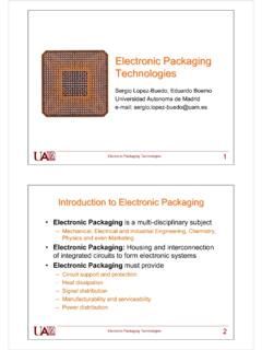
Electronic Packaging Technologies - Carleton University
www.doe.carleton.caChip Scale Packages (CSP) • Chip Scale Package, or CSP, based on IPC/JEDEC J-STD-012 definition, is a single-die, direct surface mountable package with an area of no more than 1.2 times the original die area Electronic Packaging Technologies 12 CSP Benefits and Drawbacks • CSP is not a new mounting technology, is an evolution of SMD

Semiconductors and Intel
www.intel.cominto die 7 4 5 JAPAN TO USA CHINA TO USA USA TO MALAYSIA SINGAPORE TO CHINA Silicon ingots cut into wafers Chip integrated into consumer good Bare wafer into by end product manufacturer fab wafer Consumer buys end product Die are assembled, packaged, tested Final product shipped for inventory Conceptualmap flow: (forillustrativepurposesonly)
ASSOCIATION CONNECTING ELECTRONICS INDUSTRIES …
www.ipc.orgFOREWORD This standard is intended to provide information on the generic requirements for organic printed board design. All aspects and details of the design requirements are addressed to the extent that they can be applied to the broad spectrum of those