Ceramic chip capacitors
Found 11 free book(s)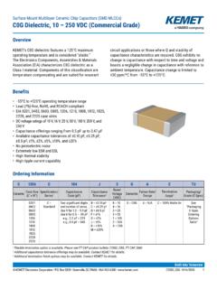
Surface Mount Multilayer Ceramic Chip Capacitors (SMD ...
content.kemet.comSurface Mount Multilayer Ceramic Chip Capacitors (SMD MLCCs) C0G Dielectric, 10 – 250 DC (Commercial Grade) Dimensions – Millimeters (Inches) L B W S T. EIA Size Code Metric Size Code. L . Length. W . Width. T . Thickness. B . Bandwidth S Separation Minimum Mounting Technique. 0201 0603 0.60 (0.024) ±0.03 (0.001) 0.30 (0.012) ±0.03 (0.001 ...
Surface Mount Multilayer Ceramic Chip Capacitors (SMD ...
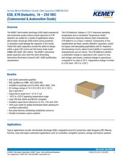
content.kemet.comSurface Mount Multilayer Ceramic Chip Capacitors (SMD MLCCs) ESD, X7R Dielectric, 16 250 VDC (Commercial & Automotive Grade) Table 1A – Capacitance Range/Selection Waterfall (cont.) Capacitance Cap Code Case Size/ Series C0805C C1206C. Rated Voltage (VDC) 16 25 50 63 100 200 250 16 25 50 63 100 200 250 Voltage Code 4 3 5. M. 1 2 A 4 3 5. M. 1 2 A
MULTILAYER CERAMIC CHIP CAPACITORS - GMC SERIES
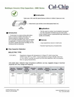
www.calchipelectronics.comMULTILAYER CERAMIC CHIP CAPACITORS - GMC SERIES - APPLICATIONS - Can be used on surface mount assembly equipment - Our fully integrated manufacturing and total quality control systems ensure unprecedented high standards of quality and reliability.

Surface Mount Multilayer Ceramic Chip Capacitors (SMD ...
content.kemet.comSurface Mount Multilayer Ceramic Chip Capacitors (SMD MLCCs) X7R Dielectric, 6.3 – 250 DC (Commercial Grade) Dimensions – Millimeters (Inches) L B W S T EIA Size Code Metric Size Code L Length W Width T Thickness B Bandwidth S Separation Minimum Mounting Technique 0402 1005 1.00 (0.040) ±0.05 (0.002) 0.50 (0.020) Solder ±0.05 (0.002) See ...
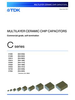
MULTILAYER CERAMIC CHIP CAPACITORS - TDK
product.tdk.comMULTILAYER CERAMIC CHIP CAPACITORS CATALOG NUMBER CONSTRUCTION (1) Series (2) Dimensions L x W (mm) (3) Temperature characteristics (4) Rated voltage (DC) (5) Nominal capacitance (pF) The capacitance is expressed in three digit codes and in units of pico Farads (pF). The first and second digits identify the first and
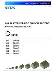
MLCC Commercial grade C series - TDK
product.tdk.comMULTILAYER CERAMIC CHIP CAPACITORS CATALOG NUMBER CONSTRUCTION (1) Series (2) Dimensions L x W (mm) (3) Temperature characteristics (4) Rated voltage (DC) (5) Nominal capacitance (pF) The capacitance is expressed in three digit codes and in units of pico Farads (pF). The first and second digits identify the first and

Cracks: The Hidden Defect - AVX Corporation
www.avx.comCracks in ceramic chip capacitors can be introduced at any process step during surface mount assembly. Thermal shock has become a “pat” answer for all of these cracks, but about 75 to 80% originate from other sources. These sources include pick and place machine centering jaws, vacuum pick up bit, board depanelization, unwarping

Part Numbering - Murata Manufacturing
search.murata.co.jp(Part Number) 1Product ID 2Series Chip Multilayer Ceramic Capacitors for General GA GC GJ GM GQ GR KR LL ZR 2 3 H 4 M A D M 3 4 J M 3 M A L A B Based on the Electrical Appliance and Material Safety Law of Japan Chip Multilayer Ceramic Capacitors for General Purpose

SURFACE-MOUNT CERAMIC MULTILAYER CAPACITORS
www.farnell.comSurface-Mount Ceramic Multilayer Capacitors 13 Product specification Y5V CONSTRUCTION Refer to table 2 to 4 Fig. 2 c 1210 3.2 4.5 For dimension see Table 1 OUUTTLINNEESS Surface mounted ultilayer ceramic apacitor dimension The capacitor consists of a rectangular block of ceramic dielectric in which a number of interleaved metal electrodes are ...
Surface Mount Ceramic Capacitor Products
catalogs.kyocera-avx.comLow Inductance Capacitors (LICC) EXAMPLE: 0612ZD105MAT2A Interdigitated Capacitors (IDC) EXAMPLE: W3L16D225MAT3A Low Inductance Decoupling Capacitor Arrays (LICA) EXAMPLE: LICA3T183M3FC4AA W 0612 2 A 4 3 Z D M W LICA 3 T 102 M 3 F C 4 A A 3 L 1 6 D 225 M A T A T 2 3 A 105 A C 103 M A T 2A Style W = RoHS L = SnPb Size 0306 0508 0612 …

Wire Bond / Ball Shear Application Note
www.knowlescapacitors.comwire. The basic steps of ball bonding include the formation of: the first bond (normally on the chip), the wire loop, and the second bond (normally on the substrate). The wire-bonding cycle is shown in Figure 1. Figure 1. Ball bonding steps. At the beginning of the wire cycle, the bonding tool travels down to the first bond location (Steps 1 ...