Digital Filter Design Using Fpga
Found 7 free book(s)
Vivado Tutorial - Xilinx
www.xilinx.comA typical design flow Objectives After completing this tutorial, you will be able to: • Create a Vivado project sourcing HDL model(s) and targeting a specific FPGA device located on the Basys3 or Nexys4 DDR boards • Use the provided user constraint file (XDC) to constrain pin locations • Simulate the design using the XSIM simulator

50 g shock NI 9237
www.ni.comNI LabVIEW FPGA Module • Design FPGA applications for NI RIO hardware • Program with the same graphical environment used for desktop and real-time applications • Execute control algorithms with loop rates up to 300 MHz • Implement custom timing and triggering logic, digital protocols, and DSP algorithms

Description Pin Assignments - Diodes Incorporated
www.diodes.com• FPGA, DSP, and ASIC Supplies • Home Audio • Network Systems • Set Top Boxes ... EN is a digital input that turns the regulator on or off. Drive EN high to turn on the regulator and low ... Connect the output LC filter from SW to the output load. Note that a capacitor is required from SW to BST to power the high-side switch. 6 .

NI 9361 Datasheet - National Instruments
www.ni.comProgrammable Digital Filter The NI 9361 has a digital filter on each of the digital input lines to filter unwanted glitches on the digital input signal. You can configure the following filter properties for each of the input lines: • Enable or disable the digital filter. • Minimum pulse width of the input signal that passes through the filter.
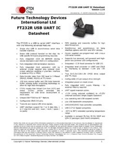
Future Technology Devices International Ltd FT232R USB ...
www.ftdichip.comexternal filter ing required. UART signal inversion option. + 3.3V (using external oscillator) to + 5.25V (internal oscillator) Single Supply Operation. Low operating and USB suspend current. Low USB bandwidth consumption. UHCI/OHCI/EHCI host controller compatible . USB 2.0 Full Speed compatible.
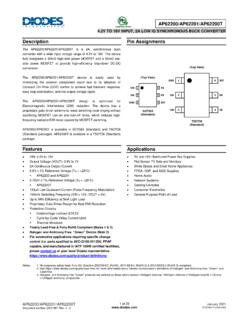
D T SW AP62200/AP62201/AP62200T 3 4 2 5 EN SW 2 5 EN …
www.diodes.comfilter from SW to the output load. GND 3 1 Power Ground. BST 4 6 High-Side Gate Drive Boost Input. BST supplies the drive for the high-side N-Channel MOSFET. A 100nF capacitor is recommended from BST to SW to power the high-side driver. EN 5 5 Enable Input. EN is a digital input that turns the regulator on or off.

Using the USB port About HS-LINK Ver. 2 - Accuphase
www.accuphase.comUsing the USB port Set to HS-LINK (Ver. 1) HS-LINK Ver. 2 Signal Transmission Block Diagram Master Clock RJ-45 Connector RJ-45 Connector Digital Audio Signal Digital Audio