Search results with tag "Fpgas"

7 Series FPGAs Configurable Logic Block User ... - Xilinx
www.xilinx.com7 Series FPGAs CLB User Guide www.xilinx.com 7 UG474 (v1.8) September 27, 2016 Preface About This Guide Xilinx® 7 series FPGAs include four FPGA fami lies that are all designed for lowest power to enable a common design to scale across families for …
UltraScale Architecture Configuration User Guide - Xilinx
www.xilinx.comXilinx FPGAs are highly flexible, reprogrammable logic devices. Like processors, Xilinx FPGAs are fully user programmable. For FPGAs, the program is called a bitstream, which defines the application-specific FPGA functionality. The bitstream loads into the FPGA internal memory at system power-up or on demand by the system.
UltraScale FPGAs Transceivers Wizard v1
www.xilinx.comUltraScale FPGAs Transceivers Wizard v1.7 7 PG182 (v1.7) December 4, 2020 www.xilinx.com Chapter 2 Product Specification The UltraScale™ FPGAs Transceivers Wizard core is the supported method of configuring and using one or more serial transceivers in a Xilinx® UltraScale or Ul traScale+™ device. In

© Copyright 2014 2021 Xilinx
china.xilinx.com2. See DS180, 7 Series FPGAs Overview, for package details. 3. GTX transceivers in FB packages support the following maximum data rates: 10.3Gb/s in FBG484; 6.6Gb/s in FBG676 and FBG900. See DS182, Kintex-7 FPGAs Data Sheet: DC and AC Switching Characteristics, for details. Optimized for Best Price-Performance (1.0V, 0.95V, 0.9V)
Kintex UltraScale FPGAs Data Sheet: DC and AC ... - Xilinx
www.xilinx.comKintex UltraScale FPGAs Data Sheet: DC and AC Switching Characteristics DS892 (v1.19) September 22, 2020 www.xilinx.com Product Specification 2 VBATT Key memory battery backup supply –0.500 2.000 V IDC Available output current at the pad –20 20 mA IRMS Available RMS output current at the pad –20 20 mA GTH and GTY Transceivers

Aurora 64B/66B v11 - Xilinx
www.xilinx.comProvided by Xilinx at the Xilinx Support web page Notes: 1. For a complete list of supported devices and configurations, see the Vivado IP catalog and associated FPGA Datasheets. 2. For more information, see the Virtex UltraScale FPGAs Data Sheet: DC and AC Switching Characteristics (DS893) [Ref1] and Kintex UltraScale FPGAs Data Sheet: DC and AC
MultiBoot with 7 Series FPGAs and SPI Application Note ...
www.xilinx.comusing SPI configuration mode. The Kintex®-7 FPGA and Micron Quad SPI serial flash on the KC705 evaluation board are used along with Vivado® Design Suite 2015.1 to demonstrate the design flow. The 7 Series FPGAs Configuration User Guide (UG470) [Ref 1] provides additional information regarding the MultiBoot feature and details on the SPI ...

These materials are © 2017 John Wiley & Sons, Inc. Any ...
www.intel.comIntroduction F ield programmable gate arrays (FPGAs) are integrated cir-cuits that enable designers to program customized digital logic in the field. FPGAs have been around since the 1980s and ... FPGA enables you to program product features and functions, adapt to new standards, and reconfigure hardware for specific

What is an SoC FPGA? - Intel
www.intel.comSoC FPGAs Available Today At present, there are three sets of SoC FPGAs available on the market, as shown in Table 1. The processors in these devices are fully dedicated, “hardened” processor subsystems (not a soft IP core implemented in the FPGA fabric). The Altera Soc FPGA model is illustrated below.
Spartan-II FPGA Family Data Sheet - Xilinx
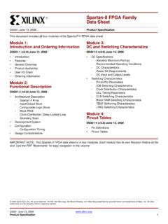
www.xilinx.comSpartan-II FPGA Family: Introduction and Ordering Information DS001-1 (v2.9) March 12, 2021 www.xilinx.com Module 1 of 4 Product Specification 3 R General Overview The Spartan-II family of FPGAs have a regular, flexible, programmable architecture of Configurable Logic Blocks (CLBs), surrounded by a perimeter of programmable Input/Output Blocks ...

Application Note HCSL Reference Clocks - CTS Corp
ctscorp.comability; the PCIe electrical interface is be-ing used in ASICs, FPGAs and SoCs. This provides designers with flexible solutions for high speed data transfer in their sys-tems. The basic PCIe architecture consists of a data link between two devices that can have 1 to 32 lanes. The lanes are differentiated as x1, x2, x4, x8, x12, x16 and x32 PCIe ...
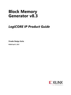
Block Memory Generator v8 - Xilinx
www.xilinx.comThe Block Memory Generator core uses embedded Block Memory primitives in Xilinx® FPGAs to extend the functionality and capability of a single primitive to memories of arbitrary widths and depths. Sophisticated algorithms within the Block Memory Generator core produce optimized solutions to provide convenient access to memories for a wide

POWEREDGE R740 - Dell
i.dell.comdouble-width or four single-width FPGAs. With up to 16 2.5” drives or 8 3.5” drives the R740 provides the versatility to adapt to virtually any application and provides the perfect platform for VDI deployments. • Scale your VDI deployments with 3 double-width GPUs, supporting up to 50% more users when compared to R730.

POWEREDGE R940xa - Dell
i.dell.comR940xa SPEC SHEET R940xaSpec Sheet 2019 Dell Inc. or its subsidiaries. ... • Choosing up to 4 double-width GPUs or up to 4 double-width or 8 single-width FPGAs for application acceleration. • Supporting large data sets with up to 48 DIMMs (24 of which can be PMems) and up to 15.36TB

Xilinx XAPP583 Using a Microprocessor to Configure Xilinx ...
www.xilinx.comUG470, 7 Series FPGAs Configuration User Guide for more details. Data Formatting and Bit-Swapping Because the configuration bitstream is loaded into memory connected to the processor, it must be formatted in a way that the processor (or another device that programs the memory) can use.

Chapter 4: Programmable Logic Devices 4.1 Chapter Overview
www.csun.edu(FPGAs) both having their advantages and disadvantages with respect to the specific ... be as high as 7.5 ns on devices that have 100 pins and 128 macrocells. ... Atmel’s 6000 series and Lucent technologies’ ORCA series. Channel-array-based devices are register rich, have many I/Os and have programmable interconnects between the logic ...
2021 - microsite-wx-industries.nvidia.cn
microsite-wx-industries.nvidia.cn目前的智能网卡有ASIC、FPGA和片上系统(SoC)三种实现。 智能网卡不同技术实现示意图 图2 智能网卡架构示意图 图3 数据来源:公开资料, 赛迪顾问整理 2021,11 数据来源:Vmware官网,赛迪顾问整理 2021,11

50 g shock NI 9237
www.ni.comNI LabVIEW FPGA Module • Design FPGA applications for NI RIO hardware • Program with the same graphical environment used for desktop and real-time applications • Execute control algorithms with loop rates up to 300 MHz • Implement custom timing and triggering logic, digital protocols, and DSP algorithms

Digital Circuit Design Using Xilinx ISE Tools
personal.utdallas.eduXilinx Tools is a suite of software tools used for the design of digital circuits implemented using Xilinx Field Programmable Gate Array (FPGA) or Complex Programmable Logic Device (CPLD). The design procedure consists of (a) design entry, (b) synthesis and

CompTIA Security+ Certification Exam Objectives
comptiacdn.azureedge.net- Field-programmable gate array (FPGA) - Arduino • Supervisory control and data acquisition (SCADA)/industrial control system (ICS) - Facilities - Industrial - Manufacturing - Energy ... (SoC) • Communication considerations - 5G - Narrow-band - Baseband radio - Subscriber identity module (SIM) cards - Zigbee • Constraints - Power ...

Quartus® Prime はじめてガイド
www.macnica.co.jp5. Family, Device & Board Settings ページでは、使用する開発キットに搭載されているインテル FPGA の型 番を選択します。 Family, Device & Board Settings ページ Board Device Family Package Pin count Core speed grade Available devices MAX fi10 FPGA Evaluation Kit MAX 10 EQFP 144 8 10M08SAE144C8G

FPGA搭載ハードIPを用いたPCIExpress構築 PCI Express Gen3 …
www.avaldata.co.jpFPGA搭載PCI Express Hard IPの理解 FPGAでPCI Expressを実現に必要なこと② Hard IPで出来ること・出来ないこと 必要とされる機能 対応 物理層 全て データリンク層 全て トランザクション層 フロー制御 MSI-X割り込み 上記以外 アプリケーション層 TLP生成/解析 ×

Spartan-6 FPGA Clocking Resources - Xilinx
www.xilinx.comSpartan-6 FPGA Clocking Resources www.xilinx.com UG382 (v1.10) June 19, 2015 02/16/2011 1.5 Added BUFGMUX routing restrictions for DCM and PLL programming clock and BUFGMUX ASYNC usage to Clock Buffers and Multiplexers.

AC 20-152 - RTCA, Inc., Document RTCA/DO-254, Design ...
www.faa.govapplication specific integrated circuits (ASIC), programmable logic devices (PLD), field programmable gate arrays (FPGA), or similar electronic components used in the design of aircraft systems and equipment. This AC provides a means (but is not the only means) to gain

Xilinx DS099 Spartan-3 FPGA Family data sheet
www.xilinx.comSpartan-3 FPGA Family: Introduction and Ordering Information DS099 (v3.1) June 27, 2013 www.xilinx.com Product Specification 4 power, the configuration data is written to the FPGA using any of five different modes: Master Parallel, Slave Parallel, Master
0.8 A, Low V , Low Dropout Linear Regulator Data Sheet ...
www.analog.comfor regulation of nanometer FPGA geometries operating from output allows power system monitors to check the health of the 2.5 output voltage.V down to 1.8 V …

Introduction to Labview - Michigan State University
www.egr.msu.eduIntroduction to Labview • Product of National Instruments (NI) • Software for Virtual Instrumentation • Data Acquisition (DAQ) • Graphical Programming • Data Storage and Analysis for wide Range of Applications. Features of LabVIEW • Design – Signal and Image Processing – Embedded System Programming • (PC, DSP, FPGA ...

Semiconductors and Intel
www.intel.comAn introduction. Semiconductors and Intel 22 Table of contents What is a semiconductor? GO Semiconductors are everywhere GO ... FPGA Field-programmable gate array; software-configurable circuits What do they do: Acceleration, communications, circuit …

Lecture 11: RISC-V - University of California, Berkeley
inst.eecs.berkeley.eduEE141 Project Introduction You will design and optimize a RISC-V processor Phase 1: Design and demonstrate a processor Phase 2: ASIC Lab – implement cache memory and generate complete chip layout FPGA Lab – Add video display and graphics
インテル® FPGA 製品カタログ - Intel
www.intel.co.jpDSP Builder for インテル® FPGA 71 インテル® FPGA SDK for OpenCL™ 72 インテル® SoC FPGA エンベデッド開発スイート 73 SoC FPGA オペレーティング・システムのサポート 74 Nios® IIプロセッサー 75 Nios® IIプロセッサー・エンベデッド・デザイン・スイート 76

DE0-CV User Manual w ww .terasic - Intel
www.intel.comApr 21, 2016 · The program will call Quartus II tools to download the control circuit to the FPGA board through the USB-Blaster[USB-0] connection. To activate the Control Panel, perform the following steps: 1. Make sure Quartus II 14.0 or a later version is installed successfully on your PC. 2. Set the RUN/PROG switch to the RUN position. 3. Connect the USB ...

FPGAのコンフィグレーション 基礎知識 《Altera編》 …
www.cqpub.co.jpFPGA(Field Programmable Gate Array)を使用する ... (AP ファーストPOR) (Intel社の特定品種) - 0 1 1 0 1.8V アクティブ・パラレル×16 フラッシュ・メモリ ...
Lab 3 : Dataflow and Behavioral Modeling of Combinational ...
people.cs.georgetown.edu5. Implement the design and program the FPGA. Verify that the circuit functioning correctly. B. Dataflow modeling of Multiplexer Enter the dataflow description of quadruple 2-to-1 multiplexer in Xilinx ISE 8.2i, and write a HDL stimulus module to simulate and verify the circuit. C. Behavioral modeling of Multiplexer 1.
FPGA Architecture White Paper - Intel
www.intel.comor fewer inputs. Therefore, a 5-LUT/2-LUT combination is also available. One Stratix II ALM can be configured to implement a 5-LUT and a 4-LUT. One of the inputs is shared between the 2 LUTs. The 5-LUT has up to 4 independent inputs. The 4-LUT has up to 3 independent inputs. The sharing of inputs between LU Ts is very common in FPGA designs ...
Similar queries
7 Series FPGAs, Xilinx, UltraScale Architecture Configuration User Guide, User, FPGA, FPGAs, Configuring, 7 FPGAs, Configuration, 7 Series FPGAs Configuration User, Introduction, What is an SoC FPGA, Intel, II FPGA Family, II family, Interface, Solutions, Memory, POWEREDGE R940xa, Sheet, Data, Series FPGAs, Series, NI 9237, Design FPGA, Digital, Design, Field Programmable Gate Array, CompTIA Security+ Certification Exam, Field-programmable gate array, Quartus® Prime, Family, PCI Express Gen3, Spartan-6 FPGA Clocking Resources, Spartan-6 FPGA Clocking Resources www.xilinx.com, Programmable, Field programmable gate arrays FPGA, FPGA Family, Dropout Linear Regulator Data Sheet, FPGA Field-programmable gate array, RISC-V, FPGA SDK for OpenCL, DE0-CV User Manual, Download, Module