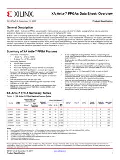
Transcription of 0.8 A, Low V , Low Dropout Linear Regulator Data Sheet ...
1 A, Low VIN, Low Dropout Linear Regulator data Sheet ADP1752/ADP1753 FEATURES Maximum output current: A Input voltage range: V to V Low shutdown current: <2 A Very low Dropout voltage: 70 mV at A load Initial accuracy: 1% Accuracy over line, load, and temperature: 2% 7 fixed output voltage options with soft start V to V (ADP1752) Adjustable output voltage option with soft start V to V (ADP1753) High PSRR 65 dB at 1 kHz 65 dB at 10 kHz 54 dB at 100 kHz 23 V rms at V output Stable with small F ceramic output capacitor Excellent load and line transient response Current-limit and thermal overload protection Power-good indicator Logic-controlled enable Reverse current protection APPLICATIONS Server computers Memory components Telecommunications equipment Network equipment DSP/FPGA/microprocessor supplies Instrumentation equipment/ data acquisition systems TYPICAL APPLICATION CIRCUITS TOP VIEW(Not to Scale)ADP17521234 VINVIN100k FVIN = = Figure 1.
2 ADP1752 with Fixed Output Voltage, V TOP VIEW(Not to Scale)ADP17531234 VINVIN100k FVIN = = (1 + R1/R2)VINEN1211109 VOUTVOUTVOUTADJ5678 PGGNDSSNCPG16151413 VINVINVOUTVOUT10nFR2R107718-002 Figure 2. ADP1753 with Adjustable Output Voltage, V to V GENERAL DESCRIPTION The ADP1752/ADP1753 are low Dropout (LDO) CMOS Linear regulators that operate from V to V and provide up to 800 mA of output current. These low VIN/VOUT LDOs are ideal for regulation of nanometer FPGA geometries operating from V down to V I/O rails, and for powering core voltages down to V. Using an advanced proprietary architecture, they provide high power supply rejection ratio (PSRR) and low noise, and achieve excellent line and load transient response with only a small F ceramic output capacitor.
3 The ADP1752 is available in seven fixed output voltage options. The ADP1753 is the adjustable version, which allows output voltages that range from V to V via an external divider. The ADP1752/ADP1753 allow an external soft start capacitor to be connected to program the startup. A digital power-good output allows power system monitors to check the health of the output voltage. The ADP1752/ADP1753 are available in a 16-lead, 4 mm 4 mm LFCSP, making them not only very compact solutions, but also providing excellent thermal performance for applications that require up to 800 mA of output current in a small, low profile footprint. Rev. H Document Feedback Information furnished by Analog Devices is believed to be accurate and reliable. However, no responsibility is assumed by Analog Devices for its use, nor for any infringements of patents or other rights of third parties that may result from its use.
4 Specifications subject to change without notice. No license is granted by implication or otherwise under any patent or patent rights of Analog Devices. Trademarks and registered trademarks are the property of their respective owners. One Technology Way, Box 9106, Norwood, MA 02062-9106, Tel: 2008 2015 Analog Devices, Inc. All rights reserved. Technical Support ADP1752/ADP1753 data Sheet TABLE OF CONTENTS Features .. 1 Applications .. 1 Typical Application Circuits .. 1 General Description .. 1 Revision History .. 2 Specifications .. 3 Input and Output Capacitor, Recommended Specifications .. 4 Absolute Maximum Ratings .. 5 Thermal data .. 5 Thermal Resistance .. 5 ESD Caution .. 5 Pin Configurations and Function Descriptions .. 6 Typical Performance Characteristics.
5 7 Theory of Operation .. 11 Soft Start Function (ADP1752/ADP1753) .. 11 Adjustable Output Voltage (ADP1753) .. 12 Enable Feature .. 12 Power-Good Feature .. 12 Reverse Current Protection Feature .. 13 Applications Information .. 14 Capacitor Selection .. 14 Undervoltage Lockout .. 15 Current-Limit and Thermal Overload Protection .. 15 Thermal Considerations .. 15 PCB Layout Considerations .. 18 Outline Dimensions .. 19 Ordering Guide .. 19 REVISION HISTORY 1/15 Rev. G to Rev. H Changes to Ordering Guide .. 19 4/14 Rev. F to Rev. G Changes to Figure 1 and Figure 2 .. 1 Change to Table 4 .. 5 Changes to Figure 3 and Figure 4 .. 6 Updated Outline Dimensions .. 19 Changes to Ordering Guide .. 19 1/14 Rev. E to Rev. F Changes to Ordering Guide .. 19 6/13 Rev. D to Rev. E Changed Adjustable Output Voltage Option with Soft Start (ADP1755) from V to V to V to V (Throughout).
6 1 Updated Outline Dimensions .. 19 12/12 Rev. C to Rev. D Added Junction Temperature of 150 C, Table 3 .. 5 9/12 Rev. B to Rev. C C h a n g e s t o Table 3 .. 5 Changes to Ordering Guide .. 19 2/10 Rev. A to Rev. B Changes to Table 4 .. 5 Changes to Ordering Guide .. 19 4/09 Rev. 0 to Rev. A Changes to Adjustable Output Voltage Accuracy (ADP1753) Parameter, Table 1 .. 3 Changes to Table 3 .. 5 10/08 Revision 0: Initial Version Rev. H | Page 2 of 20 data Sheet ADP1752/ADP1753 SPECIFICATIONS VIN = (VOUT + V) or V (whichever is greater), IOUT = 10 mA, CIN = COUT = F, TA = 25 C, unless otherwise noted. Table 1. Parameter Symbol Test Conditions/Comments Min Typ Max Unit INPUT VOLTAGE RANGE VIN TJ = 40 C to +125 C V OPERATING SUPPLY CURRENT1 IGND IOUT = 500 A 90 A IOUT = 100 mA 400 A IOUT = 100 mA, TJ = 40 C to +125 C 800 A IOUT = A mA IOUT = A, TJ = 40 C to +125 C mA SHUTDOWN CURRENT IGND-SD EN = GND, VIN = V 2 6 A EN = GND, VIN = V, TJ = 40 C to +85 C 30 A EN = GND, VIN = V, TJ = 40 C to +85 C 100 A OUTPUT VOLTAGE ACCURACY Fixed Output Voltage Accuracy (ADP1752) VOUT IOUT = 10 mA 1 +1 % IOUT = 10 mA to A + % 10 mA < IOUT < A, TJ = 40 C to +125 C 2 +2 % Adjustable Output Voltage Accuracy (ADP1753)
7 2 VADJ IOUT = 10 mA V IOUT = 10 mA to A V 10 mA < IOUT < A, TJ = 40 C to +125 C V LINE REGULATION VOUT/ VIN VIN = (VOUT + V) to V, TJ = 40 C to +125 C + %/V LOAD REGULATION3 VOUT/ IOUT IOUT = 10 mA to A, TJ = 40 C to +125 C %/A Dropout VOLTAGE4 VDROPOUT IOUT = 100 mA, VOUT V 10 mV IOUT = 100 mA, VOUT V, TJ = 40 C to +125 C 16 mV IOUT = A, VOUT V 70 mV IOUT = A, VOUT V, TJ = 40 C to +125 C 140 mV S TA R T-UP TIME5 tS TART-UP CSS = 0 n F, IOUT = 10 mA 200 s CSS = 10 nF, IOUT = 10 mA ms CURRENT-LIMIT THRESHOLD6 ILIMIT 1 5 A THERMAL SHUTDOWN Thermal Shutdown Threshold TSSD TJ rising 150 C Thermal Shutdown Hysteresis TSSD-HYS 15 C PG OUTPUT LOGIC LEVEL PG Output Logic High PGHIGH V VIN V, IOH < 1 A V PG Output Logic Low PGLOW V VIN V.
8 IOL < 2 mA V PG Output Delay from EN Transition Low to High V VIN V, CSS = 10 nF ms PG OUTPUT THRESHOLD Output Voltage Falling PGFA L L V VIN V 10 % Output Voltage Rising PGRISE V VIN V % EN INPUT EN Input Logic High VIH V VIN V V EN Input Logic Low VIL V VIN V V EN Input Leakage Current VI- LEAKAGE EN = VIN or GND 1 A UNDERVOLTAGE LOCKOUT UVLO Input Voltage Rising UVLORISE TJ = 40 C to +125 C V Input Voltage Falling UVLOFA L L TJ = 40 C to +125 C V Hysteresis UVLOHYS TJ = 25 C 100 mV SOFT START CURRENT ISS V VIN V A ADJ INPUT BIAS CURRENT (ADP1753) ADJI- BIAS V VIN V, TJ = 40 C to +125 C 10 150 nA SENSE INPUT BIAS CURRENT SNSI- BIAS V VIN V 10 A Rev.
9 H | Page 3 of 20 ADP1752/ADP1753 data Sheet Parameter Symbol Test Conditions/Comments Min Typ Max Unit OUTPUT NOISE OUTNOISE 10 Hz to 100 kHz, VOUT = V 23 V rms 10 Hz to 100 kHz, VOUT = V 65 V rms POWER SUPPLY REJECTION RATIO PSRR VIN = VOUT + 1 V, IOUT = 10 mA 1 kHz, VOUT = V 65 dB 1 kHz, VOUT = V 56 dB 10 kHz, VOUT = V 65 dB 10 kHz, VOUT = V 56 dB 100 kHz, VOUT = V 54 dB 100 kHz, VOUT = V 51 dB 1 Minimum output load current is 500 A. 2 Accuracy when VOUT is connected directly to ADJ. When VOUT voltage is set by external feedback resistors, absolute accuracy in adjust mode depends on the tolerances of resistors used. 3 Based on an end-point calculation using 10 mA and A loads. See Figure 6 for typical load regulation performance.
10 4 Dropout voltage is defined as the input to output voltage differential when the input voltage is set to the nominal output voltage. This applies only to output voltages above V. 5 Start-up time is defined as the time between the rising edge of EN to VOUT being at 95% of its nominal value. 6 Current-limit threshold is defined as the current at which the output voltage drops to 90% of the specified typical value. For example, the current limit for a V output voltage is defined as the current that causes the output voltage to drop to 90% of V, or V. INPUT AND OUTPUT CAPACITOR, RECOMMENDED SPECIFICATIONS Table 2. Parameter Symbol Test Conditions/Comments Min Typ Max Unit MINIMUM INPUT AND OUTPUT CAPACITANCE1 CMIN TA = 40 C to +125 C F CAPACITOR ESR RESR TA = 40 C to +125 C 1 The minimum input and output capacitance should be greater than F over the full range of operating conditions.