Low Voltage Current Loop Transmitter
Found 9 free book(s)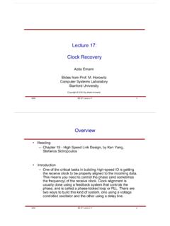
Lecture 17: Clock Recovery - Stanford University
web.stanford.edu(transmitter clock is sent along with the data) • The basic circuit block is a Phase Locked Loop ... • Main goal is to achieve low offset • Loop filters ... whose value is adjusted by the control voltage/current: • Main problem: Create a “resistor” that is both variable AND linear ctrl load o+ o …

NELES® ND9000 INTELLIGENT VALVE CONTROLLER
www.valin.comSupply power: Loop powered, 4–20 mA Minimum signal: 3.6 mA Current max : 120 mA Load voltage: up to 9.7 VDC/20 mA (corresponding 485 Ω) Voltage: max. 30 VDC Polarity protection: -30 VDC Over current protection: active over 35 mA Profibus PA and FOUNDATION fieldbus Supply power: voltage 9–32 VDC, reverse polarity protection
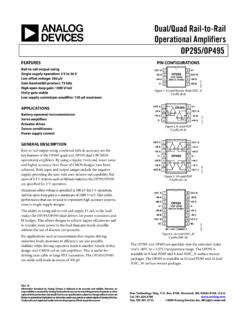
Dual/Quad Rail-to-Rail Operational Amplifiers OP295/OP495
www.analog.comLow offset voltage: 300 μV . Gain bandwidth product: 75 kHz . High open-loop gain: 1000 V/mV . Unity-gain stable . Low supply current/per amplifier: 150 μA maximum . APPLICATIONS . Battery-operated instrumentation . Servo amplifiers . Actuator drives . Sensor conditioners . Power supply control . GENERAL DESCRIPTION

Kinetis K66 Sub-Family - NXP
www.nxp.comSymbol Description Min. Max. Unit VDD Digital supply voltage –0.3 3.8 V IDD Digital supply current — 300 mA VDIO Digital1 input voltage,including RESET_b –0.3 VDD + 0.3 V VAIO Analog1 input voltage, including EXTAL32 and XTAL32 –0.3 VDD + 0.3 V ID Maximum current single pin limit (digital output pins) –25 25 mA VDDA Analog supply voltage VDD – 0.3 VDD + …

MCP2561/2FD High-Speed CAN Flexible Data Rate Transceiver
ww1.microchip.comapplying high-level voltage to the STBY pin. In Standby mode, the transmitter and the high-speed part of the receiver are switched off to minimize power consumption. The low-power receiver and the wake-up filter blocks are enabled to monitor the bus for activity. The receive pin (R

Rosemount 3051 Pressure Transmitter - Emerson Electric
www.emerson.com3.1.5 In-line gage transmitter orientation. The low side pressure port (atmospheric reference) on the in-line gage transmitter is located in the neck of the transmitter, behind the housing. The vent path is 360° around the transmitter between the housing and sensor. (See Figure 3-6) Keep the vent path free of any obstruction, including but not ...
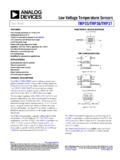
Low Voltage Temperature Sensors Data Sheet …
www.analog.comLow Voltage Temperature Sensors Data Sheet TMP35/TMP36/TMP37 FEATURES Low voltage operation (2.7 V to 5.5 V) S Calibrated directly in °C . 10 mV/°C scale factor (20 mV/°C on . TMP37) ±2°C accuracy over tempe rature (typ) ±0.5°C linearity (typ) Stable with large capacitive loads . Specified −40°C to +125°C, operation to +150°C

28/40/44-Pin, Low-Power, High-Performance Microcontrollers ...
ww1.microchip.com- Fixed Voltage Reference (FVR) with 1.024V, 2.048V and 4.096V output levels - 5-bit rail-to-rail resistive DAC with positive and negative reference selection • Charge Time Measurement Unit (CTMU) module: - Supports capacitive touch sensing for touch screens and capacitive switches eXtreme Low-Power Features (XLP) (PIC18(L)F2X/4XK22):

MC68HC908GP32, MC68HC908GP32 - Data Sheet - NXP
www.nxp.comMC68HC908GP32 Data Sheet, Rev. 10 Freescale Semiconductor 5 January, 2008 10 Figure 13-5. SCI Receiver Block Diagram — Replaced SCI receiver block diagram