Protective Semiconductor
Found 9 free book(s)
Fabrication of Semiconductor Devices
www-physics.lbl.govProtective layers immediately adjacent to the active semiconductor bulk must form a well controlled interface to the semiconductor lattice, to 1. minimize additional charge states (“dangling” bonds) 2. avoid mechanical stress (mismatch of thermal expansion coefficients) In these respects SiO 2 on Si is unequalled – indeed this is probably

The Semiconductor Supply Chain: Assessing National ...
cset.georgetown.eduSemiconductor fabrication facilities (“fabs”) make chips in these wafers in two steps: forming transistors and other electrical devices in material layers within ... and enclosed in a protective casing. This produces the final look of a dark gray rectangle with metal pins at the edges (third image in Figure 2). The chip is also tested to ...

Chapter 1 Introduction to Chemical Vapor Deposition (CVD)
www.asminternational.orgconcentrate on compound semiconductor applications. The book by Kodas and Hampden-Smith9 and the series of proceedings volumes, represented by Sandhu et al. 10 focus on CVD of ... protection, and chapter 14 discusses protective CVD coatings for tool steels. Chapter 10 discusses the CVD of diamond, and diamond-

Hall Effect Experiment Manual
d2n0lz049icia2.cloudfront.netIndividual protective equipment must be used to prevent shock and arc blast injury where hazardous live conductors are exposed. ... the semiconductor is immersed in the magnetic field transverse to the direction of flow of current. The moving charge experiences aLorentz force:

ON Semiconductor Is Now
www.onsemi.comAlso included are protective features consisting of input and reference undervoltage lockouts each with hysteresis, cycle−by−cycle current limiting, programmable output deadtime, and a latch for single pulse metering. These devices are available in an 8−pin dual−in−line plastic package as well as the 14−pin plastic surface mount ...

ON Semiconductor Is Now
www.onsemi.comAlso included are protective features consisting of input and reference undervoltage lockouts each with hysteresis, cycle−by−cycle current limiting, a latch for single pulse metering, and a flip−flop which blanks the output off every other oscillator cycle, allowing output dead times to be programmed for 50% to 70%.
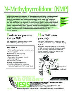
N-Methylpyrrolidone(NMP) (NMP) - CDPH Home
www.cdph.ca.govprotective utility gloves such as butyl rubber or Silvershield® (laminated polyethylene/EVOH) when using products that contain NMP. NMP will go right through less durable gloves such as those made of natural rubber, nitrile, or polyethylene. Replace gloves often. Use chemical protective clothing such as aprons, sleeves, boots, and head

Yield and Yield Management - Smithsonian Institution
smithsonianchips.si.edusemiconductor industry. Line yield refers to the number of good wafers produced with-out being scrapped, and in general, measures the effectiveness of material handling, process control, and labor. Die yield refers to the number of good dice that pass wafer probe testing from wafers that reach that part of the process. It is intended to prevent

Chapter 5 Protection Circuit Design
www.fujielectric.comprotective circuit built in, thereby simplifying the drive circuit design. For more details, refer to Chapter 7 “Drive Circuit Design”. Fig. 5-4 shows an IGBT waveform during short circuit protection. + +